| T O P I C R E V I E W |
| Ramon.Haemmerle |
Posted - 30 Jun 2017 : 09:35:43
Hello guys,
Does someone know a good solution for moving STEP Files / 3D Files in Z - Direction.
Most likly i am talking about GAP PADS which should be on top of a Part.
Lets say the Part is 5mm high and i would like to place the GAP PAD on top of it.
Next time the same GAP PAD will be on top of a 8mm Part. Now i would have to make
a new GAP PAD (3D File) all the time with a different koordinate system. Which makes it timeintense and
complicated if you are using a lot of different GAP PAD´s.
Would there be a reason to implement this function in the next version ?
Or is there allready something like that ?
I know you can move it in the Footprint Editor but this is not a great solution, as many different Parts
can have the same Footprint and not every GAP PAD has the same movement in Z.
Maybe we can find some people which are intrested in this function aswell ??
Would appreciate any help I can get!
Thank you !
best regards,
Ramon |
| 9 L A T E S T R E P L I E S (Newest First) |
| steve |
Posted - 14 Jul 2017 : 08:53:38
As stated, we are looking to advance the 3D environment in a future Major release. for now we are concentrating on our next intermediate release V9.1 and others planned for our recent Major release V9.
News of fututre releases will come via your local distributor.
Pulsonix Assistance |
| Ramon.Haemmerle |
Posted - 14 Jul 2017 : 07:22:21
Hello steve,
Thank you a lot.
Can you already tell me a date for the release ?
Or do you have no Plans yet ?
regards
Ramon |
| steve |
Posted - 13 Jul 2017 : 16:51:07
Extensions to 3D operation are on our roadmap for the next major release, and all enhancement requests in this area - including your request which has been logged on our support database - will be reviewed as part of that project.
Pulsonix Assistance |
| Ramon.Haemmerle |
Posted - 13 Jul 2017 : 13:44:48
Hello guys,
I guess no one has a solution for our problem ?
Can we get a Statement from an Administrator ?
Will there be a solution ? We thought this problem will be fixxed in V9.x.
best regards,
Ramon |
| Ramon.Haemmerle |
Posted - 05 Jul 2017 : 14:01:44
Hallo Jameshead,
Yeah i understood that.
But we are using the Function "STEP - No Model Transformations".
Not sure if you know that Function ? It is mainly for the STEP Files:
Normally Pulsonix takes the Part and makes a frame around it.
For placing the STEP File the programm takes the middle of this frame and places
the STEP File there and as we do not have the coordinate system in the middle in each part,
we need to use it. Same with the rotation (0°,90°,180°,...).
So this one does not work and that is the actuell problem which we have.
Sorry for not sharing this information before, with you.
best regards,
Ramon |
| jameshead |
Posted - 05 Jul 2017 : 13:50:34
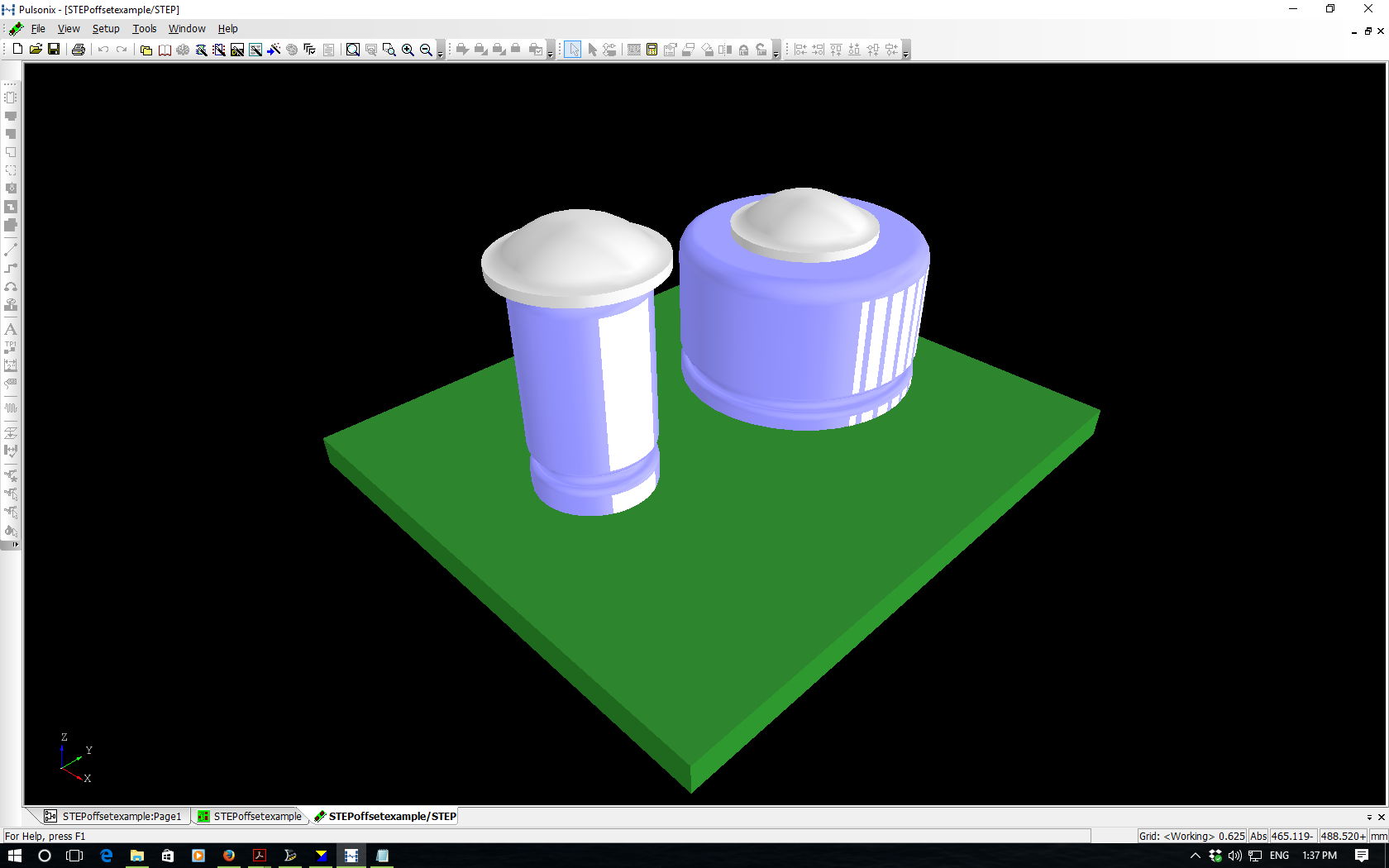
Here's an example board with two capacitors C1 having a component height of 11.20mm and C2 having a component height of 8.30mm. Both have associated STEP models.
Both have the same 3M stick-on foot to provide insulation on the metal top surface of the electrolytic capacitor. The part is 3M SJ-5302TRANS and has a footprint with a linked step model.
The default value for the 3M provided step model is:
<STEP Offset> is "X=-6.40;Y=0.00;Z=11.20mm"
This value has been edited in the PCB using Edit Attributes so that:
C1A is X=-6.40;Y=0.00;Z=11.20mm as C1 is 11.20mm high
C2A is X=-6.40;Y=0.00;Z=8.30mm as C2 is 8.30mm high
Image Insert:
119.39 KB
Download Attachment:  STEP_Offset_Example.zip STEP_Offset_Example.zip
85.57 KB |
| jameshead |
Posted - 05 Jul 2017 : 13:20:18
Hi Ramon,
What I was getting at is you have a resistor say R1 that has a component height of 1mm, and another resistor R2 that has a component height of 2mm, plus they have associated step files.
You add a part to the library for the gap pad, with its associated step file, that has the normal step offset of X=0;Y=0;Z=0 or you may just leave it blank.
When you add your gap pads to your PCB and schematic, called for example R1A and R2A, they will come in from the library with the <Step Offset> being X=0;Y=0;Z=0
In the PCB editor place the relevant gap pads over the relevent components then select from the menu Edit Attributes, scroll down to find the Gap pads in the list and scroll across to find the <Step Offset> attribute, then enter X=0;Y=0;Z=1mm for R1A, and X=0;Y=0;Z=2mm for R2A. You should see the attribute change from being bold to being not bold to indicate that you've overridden the attribute value from the library. |
| Ramon.Haemmerle |
Posted - 05 Jul 2017 : 12:42:12
Hello James,
Thank you for the answer.
Yeah but this is really inconvenient.
Because i would like to use one Part Nr. 0123456 which will be placed on top of a 1.0mm Resistor.
So i will generate a STP File with offset z = Component Height.
And i would like to keep the Footprint with an Z=0 offset and would like to use STP File Z-Offset = 0 aswell
and the STEP offset is also not usefull because i can place the GAPPAD / Part: 0123456 on different Resistor´s or Capa....
So the best way to improve on this Topic:
Add a Design based Offset for this Part.
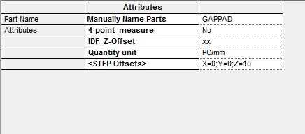
Can you maybe explain how to use the STEP Offset Attribute ?
Image Insert:
15.23 KB
Thank you for your great work.
Appreciate it a lot.
best regards,
Ramon |
| jameshead |
Posted - 30 Jun 2017 : 20:40:06
I am guessing that you mean a thermal pad stuck on the top of a component.
I have done a similar thing before with a 3M plastic stick-on cap that goes on top of Electrolytic Capacitors to prevent them from shorting out with anything.
I created a new part for the component with a schematic diagram symbol that's just a filled-in circle with no pads that's inserted near to the component it's used on. I usually name this kind of accessory, like heatsinks, using the component reference of the device it's attached to, with a letter suffix so C101 would have the stick-on insulator C101A.
The stick-on insulator has it's own PCB footprint that has it's own STEP model associated with it, and it sits on the surface of the PCB by default so Z=0.
When I add it to the PCB I edit the STEP Offset attribute for the stick-on insulator in the PCB Editor so make the Z offset equal to the <Component Height> value of the capacitor.
I use a "parts based" library so that individual parts in the library have their own unique footprint, hence I have separate footprints for each component height, using the IPC-7351C naming standard, with individual STEP files linked to individual footprints so in my library I have separate footprints for a 1.75mm SOIC than for a 1.2mm high SOIC, and the part has the <Component Height> attribute populated.
It would be useful, for the functionality you want, I think to use attribute substitution in the <STEP Offsets> attribute to refer to the <Component Height> attribute of another component. I guess for a Thermal Pad named IC10A attached to a chip IC10 that this could look something like:
X=0;Y=0;Z=%%<Component Height>{IC10}%%
or some other sensible syntax.
This would be a useful feature I agree.
As far as I know you are already able to substitue an attribute in <Step Offsets> but not for the value of an attribute on a separate component: only the same component or a design level attribute. |