Note: You must be registered in order to post a reply. To register, click here. Registration is FREE!
T O P I C R E V I E W
HarryHirn
Posted - 14 Nov 2018 : 10:21:14 Hi,
i was wondering if i am unable to find a specific option in the technology.
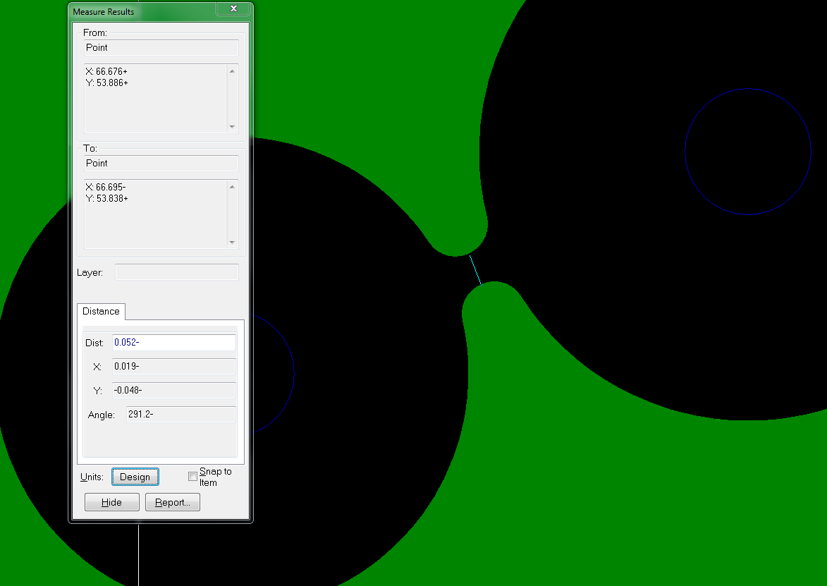
my problem: i decided to do a layout with minimum 100um structure size. in the technology file the smallest spacing rule is 100um, some are above. copper line style is 100um. the result can be seen in the picture, copper distance is 50um:
Image Insert: 40.78 KB
i absolutely understand why this happens from the rendering perspective, but is there any rule or property i can set so that pouring copper wont create structures smaller than 100um at all?
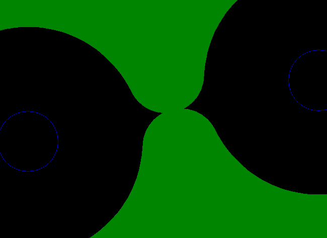
if not i suggest/request an option that will allow to define/restrict those pour copper results. this might also help prevent such things to happen:
Image Insert: 6.76 KB
4 L A T E S T R E P L I E S (Newest First)
HarryHirn
Posted - 14 Nov 2018 : 10:49:04 i think there should be such a rule to provide data to the manufacturer that keeps structures in defined limits.
psxforum
Posted - 14 Nov 2018 : 10:43:08 As the copper is all on the same net, the "spacing" rules don't really apply, those are there to keep items of different nets apart.
D.
HarryHirn
Posted - 14 Nov 2018 : 10:38:21
quote:Originally posted by psxforum
The copper shape will be poured using the line style of the 'owner' pour area. Thus it cannot create any lines or curves with a width thinner than that line style. This could explain why you cannot get those two 'noses' to touch in your first picture.
Thank you for your quick reply. I do understand why i cannot get the noses to touch.
But as i defined the minimum width as 100um i want the noses to spread apart to create a space between them of at least 100um (first picture).
That is something Pulsonix cant provide as far as i figured out, right?
Workaround might be increasing the copper line style width, but then some connection will not be closed that could easily be closed in 100um.
psxforum
Posted - 14 Nov 2018 : 10:33:26 The copper shape will be poured using the line style of the 'owner' pour area. Thus it cannot create any lines or curves with a width thinner than that line style. This could explain why you cannot get those two 'noses' to touch in your first picture.
As for the second picture, no there is no check in the application that will catch this tiny overlap, this is the kind of artefact that you would probably need to look for using third-party 'DFM' tools which know about things like acid traps.