Note: You must be registered in order to post a reply. To register, click here. Registration is FREE!
T O P I C R E V I E W
uslimey
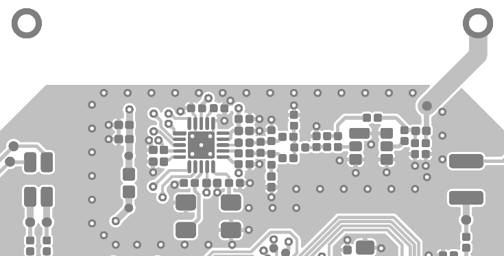
Posted - 05 Feb 2019 : 02:51:47 I have been having a host of problems producing CAM Plots in Version 10.0 Build 7247... In my panel design, despite deselecting the "plot holes in pads" option for each layer the output plots holes in all the pads... If I plot an individual design, I have been able to plot solid pads, but only in the top layer. The really crazy thing is that the top copper layer in the individual design gets plotted with the drill ident letters, which completely destroys the integrity of the board. Basically the top copper layer includes the letters that appear in the PDF files.
Has anyone else been having problems with plotting?... Am I doing something wrong?... It's so odd...
5 L A T E S T R E P L I E S (Newest First)
jameshead
Posted - 05 Feb 2019 : 07:40:46 The holes in drill plots is only present for people who are etching double-sided FR4 in Ferric Chloride and drilling the holes out with a dremel. A decent fabricator will turn the anulus to a round in the CAM tooling process though it's far better not to include them in the output.
I've set Draw Drill Holes to "By Layer Class" under options; then for Layer Classes, set Drill Hole off for Draw/Plot Appearance under Electrical
But you still may need to see holes, particulary non-plated mounting holes with no copper pads if you've created then without a copper land equal to the drill size.
Therefore I have a new layer class called Holes where the Drill Hole is turned ON for Draw/Plot Appearance, then two layers called Holes Top and Holes Bottom that can be turned on and off to display holes on the screen or not.
Another advantage of this approach is that you can create gerber outputs with correctly filled round apertures for component through-holes and vias, and a CAM Plot output for documentation in Greyscale PDF that shows the holes and copper, though you'll also need to create a colour pallette using greys, black, and white.
Image Insert: 20.18 KB
uslimey
Posted - 05 Feb 2019 : 06:50:28 Ok... Finally got it... It helps to select the Electrical Layer for turning holes off... :)
Looking back, I see the last couple of designs I did had holes in the Gerbers. I suspect the PCB house modified the G_Code accordingly... In this instance (with a panel design) they didn't like the holes... Oh well, you live and learn...
uslimey
Posted - 05 Feb 2019 : 05:42:12 Aghh...
It's still not right... The plots are fine for individual jobs, but this setting appears to be ignored for a panel design... I made sure all the PCBs in the panel had the same technology setting for filling holes... I did the same for the panel design, and it left the holes in every donut... I even tried reloading all the files... Still the same...
Any other suggestions?
I mean, if I can't fix it in software I suppose I could edit the G Code.., I notice the G Code has annulus' defined with 2 dimensions (the second being the hole), instead of circles with a single dimension.
So frustrating....
uslimey
Posted - 05 Feb 2019 : 05:15:20 Wow, that has to be the most ridiculous method of defining the way pads appear in the CAM Plot... I ran EasyPC for years... With EasyPC there is a check box in the plotting and printing dialog to fill holes - it makes perfect sense... Here it's buried in the technology file, but not where you'd expect it under the CAM Plots tab...
It's odd how the similar EasyPC and Pulsonix are in so many things, yet so different in others... Pulsonix is supposed to be the "more professional" or "high end" version of EasyPC yet some of the things they have changed make absolutely no sense. This being one of them.
Anyway, thanks for your help... I have literally spent hours digging around the help files and the technology with no luck whatsoever...
bkamen
Posted - 05 Feb 2019 : 04:55:14 I am not having that problem.
There's also a general setting for showing holes (or plotting them ) in the Electrical Class properties (See Technology->Layers->Layer Classes)
I have showing holes for pads unchecked. (don't)
And THEN in (o)ptions -> Display -> PCB Drawing -> Show Holes <Always>