| T O P I C R E V I E W |
| Sarath Chandran |
Posted - 04 May 2021 : 16:18:19
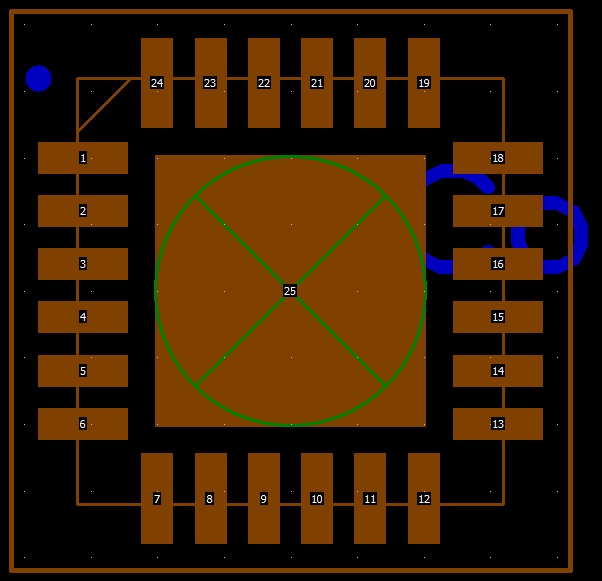
Can anyone please suggest the procedure to add thermal vias behind an IC(in the power pad area) similar to the one shown below using Pulsonix?
Image Insert:
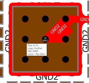
26.86 KB |
| 8 L A T E S T R E P L I E S (Newest First) |
| Sarath Chandran |
Posted - 10 May 2021 : 13:35:27
Thank you, yes you are right the one I was using have slight dimension variations. As per my datasheet (https://www.ti.com/lit/ds/symlink/bq24610.pdf?ts=1620582552156) I also need to use the same RGE0024B footprint and I can directly use what you shared :) |
| jameshead |
Posted - 05 May 2021 : 13:15:54
By the way, the footprint I posted was for a Texas Instruments DAC9881SRGET.
http://www.ti.com/lit/ds/symlink/dac9881.pdf
This is the Texas Instruments VQFN RGE0024B. You can check the TI package name against the one on your datasheet.
If you edit the footprint I sent, go to Edit and Design Properties you will see that I include attributes for my footprints detailing them.
I use PCB Libraries Footprint Expert mostly and this is a footprint I created through their software.
Image Insert:
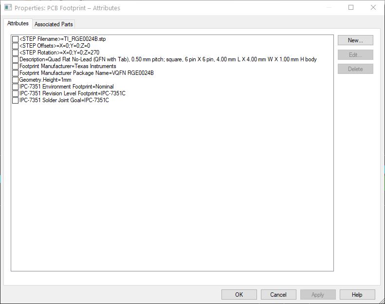
53.69 KB |
| jameshead |
Posted - 05 May 2021 : 13:09:23
The file that you are using is an older more generic one I expect. I am guessing that you got it from either SNAPEDA or Component Search Engine (Samacsys)? Both are good sources for component footprints provided you double-check against the component datasheet first.
I have found errors before on footprints from both SNAPEDA and Samacsys, and have seen them fix the errors speedily after I've reported them.
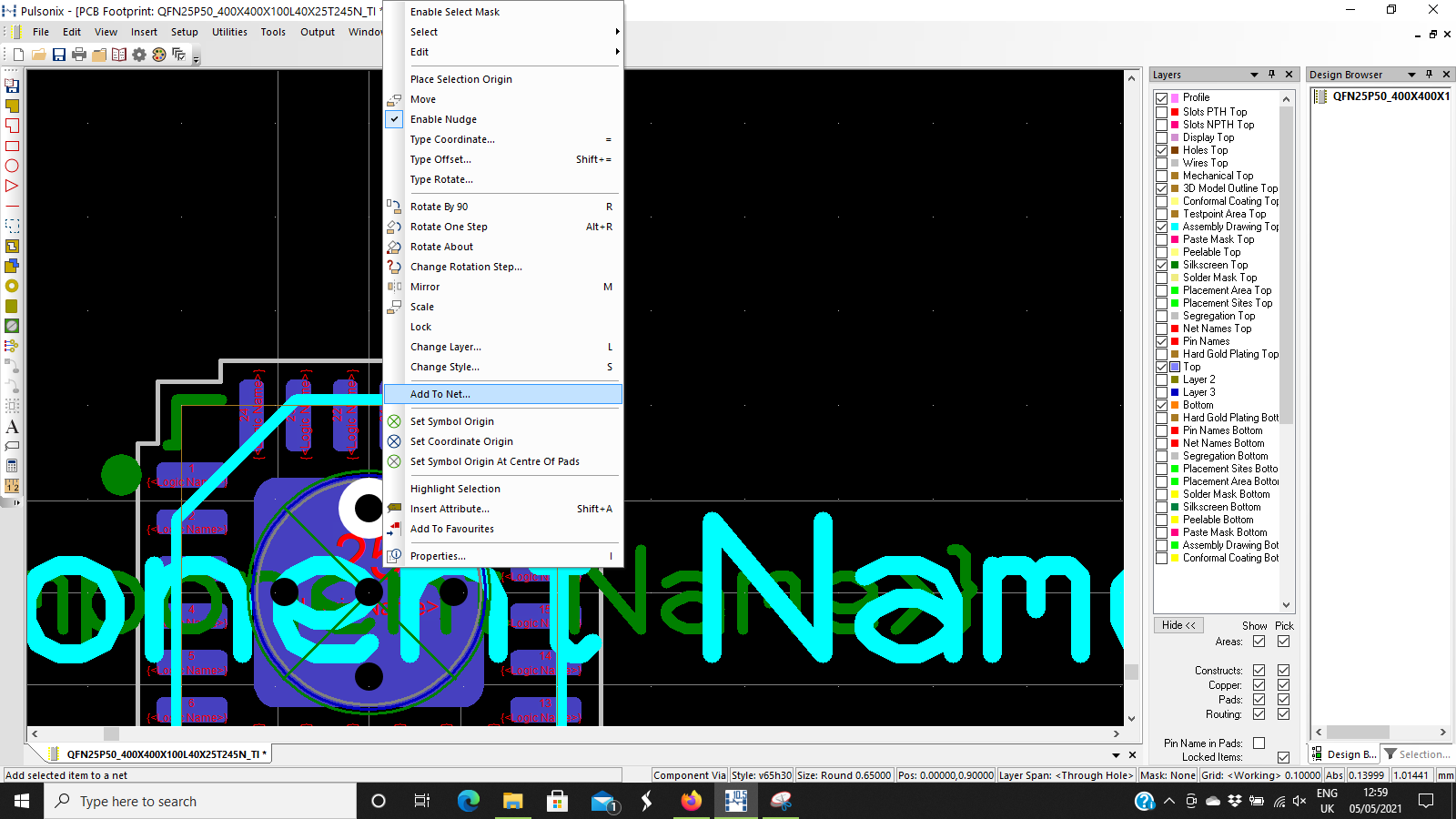
In the footprint editor, select the via, click the right mouse button, and in the menu that opens you should find Add To Net about 2/3 of the way down between Change Style and Set Symbol Origin.
If you don't see the Add To Net option on this menu then you may see instead Mark Net and Remove From Net. These menu options will tell you that the via you added is already attached to A Net. If this is the case you can use Mark Net to check which pads, mounting holes, and vias are on the same net.
Here's a picture.
Image Insert:
157.04 KB |
| Sarath Chandran |
Posted - 05 May 2021 : 11:47:02
I am using QFN50P400X400X100-25N, attached here I hope this is same as your file.
I just followed your suggestion and added vias in the thermal pad but if I right click the via I am not getting an option Add to Net to add vias to the same thermal pad net. This procedure I should do within the footprint editor itself right?
Download Attachment:  QFN50P400X400X100-25N.zip QFN50P400X400X100-25N.zip
622 Bytes
Image Insert:
88.16 KB |
| jameshead |
Posted - 05 May 2021 : 09:29:36
Apply Vias is really a tool for adding vias throughout a copper plane area, or as a fence around the PCB profile, or surrounding a track. It's not the tool I would use in your circumstance.
The benefit of adding the vias in the footprint is that you get to move the vias together, more easily, with the footprint if you are editing the board afterwards.
If you are adding vias in the footprint just open the footprint, select the thermal pad, right mouse button and select Add To Net and okay the netname which should be a number. Don't worry - it won't match the net name in your design but this doesn't matter in the footprint editor.
Use Insert Via, press S for styles to select an appropriate style for the via, pop them down in the thermal pad area, then select the vias, right mouse button, select Add to Net and add the vias to the same net name as the thermal pad.
I don't know what device or footprint you are after but here's a 25 pin (24 pin + 1 thermal pad pin) 0,50 mm pitch QFN with vias I made for a Texas Instruments part. It's in Pulsonix 10,5 format and called:
QFN25P50_400X400X100L40X25T245N_TI
QFN 25 pin, 0,5 mm pitch, 4 mm x 4 mm body, 1 mm height, pin size 0,4 mm x 0,25 mm, 2,45 mm thermal square pad, nominal density.
Download Attachment: QFN25P50_400X400X100L40X25T245N_TI.zip
85.32 KB |
| Sarath Chandran |
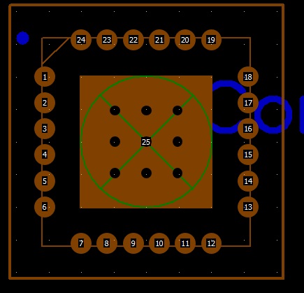
Posted - 05 May 2021 : 08:59:50
Thanks both again, you two are awesome:). I tried to add vias in footprint itself so I thought I could use this for another designs. I managed to add vias in the footprint but the IC pin pad shape also converting from square to round. See below images for the steps I followed, what could be the issue?
1.Footprint added to edit footprint page
Image Insert:
60.25 KB
2.Selected 'Apply Vias' from utilities - here you can see the outer square pads converted to round shape
Image Insert:
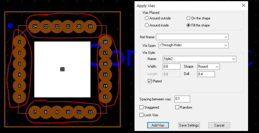
100.24 KB
3.Vias added in footprint.
Image Insert:
45.16 KB |
| jameshead |
Posted - 04 May 2021 : 16:49:48
Do want this as a permanent option in the footprint or just to add in individual PCB designs?
For the actual via, there are a couple of ways you can go about this.
If you're adding a via in the PCB design then, if you are using tented vias everywhere else, i.e. with solder mask covering the via, then the best way is enable vias for the solder mask layer class so vias have a clearance by default, then create a pad style for the vias to use in the majority part of your design and use the BY LAYER feature to make the Solder Mask pad size equal to 0 on both top and bottom sides, then to create a new pad style with the same copper land size and drill hole size, but without the BY LAYER feature to use for the thermal pad vias.
Then just pop the vias down where required, ensuring they are on the same net as the thermal pad and make sure that they are the pad style that does not have the BY LAYER for soldermask tenting.
You can add extra copper on other layers and a rectangular solder mask clearnace on the reverse side of the board if required by using Templates for extra copper and a DOC SHAPE for an extra solder mask clearance.
You can also add these vias within the footprint so that they are there permanently, or one method I used, to add the vias to the footprint as BreakOut Vias, so they can be enabled if you need them but not there if you don't. |
| bkamen |
Posted - 04 May 2021 : 16:45:57
I just use vias in the pad.
Most of the time I just add them by hand (make sure to check each via is connected to the net of the pad under the IC).
But sometimes I've been known to add them to the footprint as well as mounting holes (so they don't have a pin number)
but the vast majority of the time, I just free-hand add vias.
-Ben
-Ben
-------------------------------------------
ben@benkamen.net
http://www.benjammin.net |
|
|