Note: You must be registered in order to post a reply. To register, click here. Registration is FREE!
T O P I C R E V I E W
HarryHirn
Posted - 27 Jul 2021 : 08:34:17 Hi,
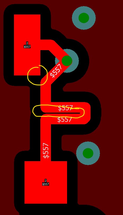
i am reworking an old design and i found several errors like that in the photo.
i am looking for a rule to show this as a DRC error, but i could not find any setting to report this. creepage seems to work only between different nets.
what i would like to get is a DRC error for same net track to track and track to pad.
Image Insert: 41.35 KB
2 L A T E S T R E P L I E S (Newest First)
lewism@pulsonix.com
Posted - 27 Jul 2021 : 17:37:38 Hi Harry,
If you are looking to suggest an enhancement please email support@pulsonix.com with the accompanying data and we will be happy to discuss options with you.
Lewis
HarryHirn
Posted - 27 Jul 2021 : 10:32:25 Ok, i found a way to show this errors, but i dont like the way it is working...
under Technology -> Net Names -> Check Same Net.
this throws a lot of unneccessary DRC
as a feature request: i would like to have a general structure rule for a whole layer. for example check layer top and dont allow structures smaller than 0.1mm for example. not between this and that and all types cross checking. as a result i can export a gerber and know that layer xy has no smaller structure than 0.1mm. thats the important thing for DFM as the manufacturer cannot produce the stencils and stuff if structures are too small.