Note: You must be registered in order to post a reply. To register, click here. Registration is FREE!
T O P I C R E V I E W
StefanThiel
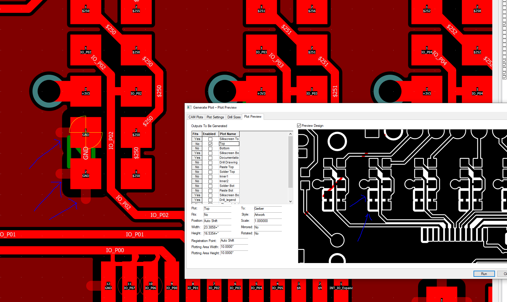
Posted - 15 Oct 2021 : 08:46:59 Hi, in the PCB my GND template is shown as connected to the pads, but in the plot output it is not. Yes, there is a Net Split Error on one of the pads, but then, the spokes should not be shown. This is very error prone, because it looks ok, but the output is differerent, and so the manufactured board is not working. best regards, Stefan
Image Insert: 155.02 KB
THIEL
2 L A T E S T R E P L I E S (Newest First)
lewism@pulsonix.com
Posted - 15 Oct 2021 : 10:17:35 Hi Stefan,
If you are able to send the design to support@pulsonix.com we can certainly investigate further for you.
Kind Regards
Lewis
jameshead
Posted - 15 Oct 2021 : 10:06:07 I can't comment on the design or the thermal ties not appearing, however I would say that it's a good idea always to output the IPC-D-356 netlist and add a note to the drawing to ask the PCB fabricator to check the translated Gerber against the supplied netlist.
To do this:
Output > Reports and select IPC-D-356 or IPC-D-356-full-metric
A note on the fabrication or drill drawing you provide may say:
Imported Gerber must be checked against supplied IPC-D-356 netlist prior to fabrication.
Bare-boards must be tested against supplied IPC-D-356 netlist or ODB++ netlist data.
Do not generate netlist for electrical test from imported Gerber data.
Any decent PCB fabricator should import your supplied netlist and compare it against the gerber they have imported to verify the design intent.
This check will often flag up intentional short circuits such as star points, intentional open circuits such as wire links or SOT-223 heatsink to middle pin etc. as well as any errors in the Gerber import process such as arcs being miss-interpreted, pads without clearance shorting to planes, or in your case, I would expect the missing thermal ties to be highlighted. The fabricator should then come back to you with the issues prior to the board being fabricated.