Note: You must be registered in order to post a reply. To register, click here. Registration is FREE!
T O P I C R E V I E W
Hobbsy
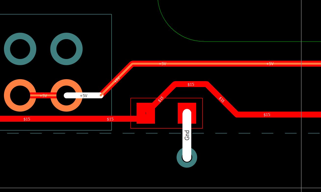
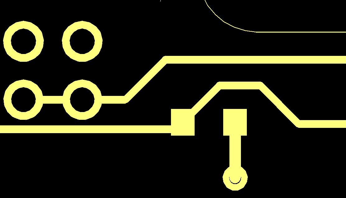
Posted - 23 Mar 2016 : 16:53:17 On either Vias or Pads that contain drill holes i can not work out with any consistency which setting or property causes the copper trace (or area) to overlap the drill hole.
See attached pictures of Pulsonix showing both tracks routed to pads/vias and then the GERBER output showing how one track overlaps the drill hole and one track does not.
Both instances occur across my design and i can't seem to isolate the issue to any of the following: - Via properties - Pad properties - Net properties - Net class properties - Track properties - Track placement or orientation
Image Insert: 71.18 KB
Image Insert: 54.21 KB
1 L A T E S T R E P L I E S (Newest First)
tystephens
Posted - 24 Mar 2016 : 09:54:17 Hi,
I've tried to repeat this and am unable to get the same results as you have, mine look as expected for vias/through hole pads, sounds like it could be settings related.
Send the design to support@pulsonix.com and they will take a look at it for you.