

The Import Design Data dialog is used for importing netlists from other EDA vendors into an existing Pulsonix PCB design.
If you wish to import a file to create a new PCB design, use the Open dialog or Data Transfer Wizard option.
As well as netlists, this mechanism can also be used to load Component Placement CSV data files to create a placed PCB. A netlist would then be applied to the placed components to complete the data. You may also wish to use this feature in conjunction with the Intelligent Gerber Import option. In addition to CSV placement files and netlists, other formats can be imported too, such as Gerber, IDF, DXF and STEP board outline files.
Locating this option
Available from: File menu > Import Design Data > choose the net format from the File Of Type list
Host System Supported Formats
Note: Some of the supported netlists appear named as PCB design netlists, this is due to the export mechanism used in the host system. Some systems require the netlist to be exported through the PCB transfer mechanism in order to collate and check the netlist for validity once in the PCB system (collation is the process of checking and amending duplicate references in the netlist e.g. duplicate component references and net names).
It should also be noted that Pulsonix does not have its own native netlist format. There are so many netlist formats out there that are already supported by Pulsonix that one of these can be used. See below for an example netlist.
Netlists and design files
- ACCEL - PCB netlist (\*.net)
- Cadstar - PCB design and netlist (\*.cpa)
- EDIF 2.0.0 netlist (\*.net)
- OrCAD EDIF netlist (\*.net)
- OrCAD II DOS PCB netlist (\*.net)
- PADS - PCB design (\*.asc)
- P-CAD - PCB design PDIF (\*.pdf \*.sd8)
- P-CAD (DOS) - PCB netlist (\*.net)
- Viewlogic Netlist EDIF netlist (\*.net)
- Viewlogic Package file netlist (\*.pkg)
Note: For PADS netlist import, use the File and Open mechanism as detailed on the PADS Netlist import page under Exporting Schematic Netlists From PADS.
For the Japan market, the Dream package is also supported. This requires a \*.net file and \*.prt file to exist. Please contact your local supplier for more information.
The Seica interface is also available for customers with this customised interface.
Other import formats
- Component Placement CSV data (\*.csv)
- DXF files (\*.dxf)
- Gerber files (\*.gbr)
- IDF files (\*.idf)
- IPC-2581 Layer stack file (\*.xml)
- STEP board outline files (\*.stp \*.step)
Importing a Design, Netlist or other format in Pulsonix PCB
From the File menu, select Import Design Data.
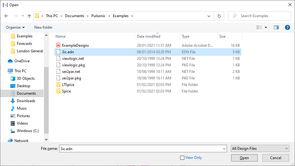
A browser opens allowing you to locate the required file:
On selection of the file, with the File of Type not preselected with the type being used, the system will automatically detect the type and then display the appropriate import dialog. This may be a Netlist, Gerber or design import dialog depending on the type detected. Any netlist being imported is checked for validity and contents during. Any errors detected are reported.
Importing a Netlist
On detection of a legal netlist, the following dialog is displayed. Each dialog is unique to the format being imported:
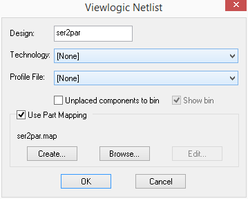
The title of the window indicates which EDA vendor that the netlist is being imported from.
Design This is the name that will be used as the basis of the filename when you save the design.
Technology This drop down list can be used to choose a technology file to base the imported design on. If you do not specify a technology file then the system defaults will be used for technology items.
Profile This drop down list allows use to specify a board profile file to use as the basis of the PCB layout that you are creating. Profiles hold items such as predefined Board outlines and Mounting holes.
Check Unplaced components to bin if you want imported components which have no position information to be placed in the Component Bin as opposed to being placed at a random position on the design.
The Show Bin option is available if the Unplaced components to bin check box has been selected. Use this option if you want the component bin to be automatically displayed after importing the netlist.
Use Part Mapping
Check Use Part Mapping to enable the part mapping option.
In general, the names used for parts in different EDA vendors systems are the same. But if there are parts that have slightly different naming system, or the other system has parts that are not in either the standard Pulsonix libraries or your own, then you can map the part names to names that exist your libraries.
Similarly you can map the footprints that you want to be used in the design.
Create will create a default mapping file for you from all the parts and footprints used in the netlist that it finds. The Save As dialog will be displayed from where you will be prompted for the name of the file that you want to save the mappings to. Initially, this will be the same name used in the Netlist for both the original name and the new mapped name. The Part Mapping Editor will then be displayed for you to change the mapping. Pressing OK will now save this file for future use or for further modification.
Browse allows you to browse for an existing part mapping file. This will load existing mappings into the Part Mapping Editor and will top up any parts that do not exist in the mapping. It will not remove any mappings and will not overwrite existing ones. Any changes to the mapping will be saved to this mapping file.
Edit allows you to re-edit an existing part mapping file.
CAE Support
Pulsonix supports CAE and Schematic systems from both a netlist and graphical file perspective.
CAE netlist files can be loaded into Pulsonix to create a PCB layout and subsequent ECO changes made. Graphical Schematics files in ASCII format can be read in to re-create the Schematics back to its original form and as it was in the host system. From the graphical files a Schematic symbol library can also be created for the items within the design if the symbol library is unavailable or missing.
The list of supported systems will change as new ones are added and supported. For a current list please contact your local sales office, our international sales office or our web site at www.pulsonix.com
Netlist Example for Import
If you wish to create a netlist by hand using a text editor, the sample netlist below can be imported into Pulsonix. This is the older OrCAD II PCB format netlist but easy to write and understand.
*ORCAD

*START

*COMP C1 "C"
*COMP R1 "Res"
*COMP U1 "AD844AN"

*NET "$1"
*NET "$1" C1."1" U1."5"

*NET "+15V"
*NET "+15V" C1."2" U1."7"

*NET "0V"
*NET "0V" R1."1" U1."3"

*END
Netlist Syntax
\*ORCAD is the mandatory file start header
\*START denotes the start of the file
Header sections use astrix \*
All internal entities are double quoted ” ”
\*COMP is the component section in the design. Component Name followed by Part Name in quotes
\*NET is the netlist. The first line is the Net Name in quotes
Each following \*NET line is the Net Name followed by the the Component Name and Pin Number (in quotes) and with a
dot separator. Each unique NET section is separated with a blank line
The Net Name can be a specified net name or a default name name using $
Once the whole netlist is finished, \*End denotes the end of the file
Related Topics
PCB Technology | PCB Profile | Open | Data Transfer Wizard | Component Bin | Part Mapping Dialog | Component Placement CSV data | Intelligent Gerber Import | Import flat Gerber | Import IDF | Import DXF | Import STEP Board Outline | IPC-2581 Layer stack file