Advanced Technology Features

Leading Edge Technology for today's modern designs

Essential functionality to support Flexi-rigid, Chip-On-Board and Embedded Component designs

Flexi-Rigid Design Support

Flexi-Rigid Technology

Flexi-Rigid Board

True Flexi-rigid support is available using the features within the Advanced Technology package; Multi-spanned Layer Areas, Board Outlines, Board Cutouts and Layer Spanned Components. Using these powerful options, Board outlines can be created to span 'internal' flexi layers that are still exposed externally.

Layer Spanned Components

Layer Spanned Component

Adding Components to layer spans allow them to be exposed. Components on inner flexi layers can be achieved but with true 'side' and layer characteristics available within their Properties. This means accurate assembly reports, manufacturing plots and precise build details can be exported for accurate manufacturing.

Advanced Layer Spans

Flexi-Rigid 3D View

Advanced layer span definitions enable you to create the regular board outline plus the board outline required for an inner flexi-layer which may extend outside of the normal board boundaries.

Embedded Component Technology

Passive Components
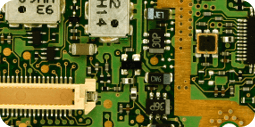
Embedded Component Technology

Passive resistors can be printed on inner layers and connected using resistive material. Depending on the manufacturing method, a resist mask or encapsulating coating will be required. Pulsonix handles this by allowing you to associate the necessary additional manufacturing layers for the resistive and other materials with the correct inner copper layer.

Buried Semiconductors and Thinned Dies
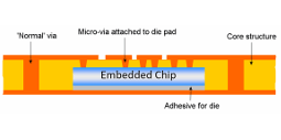
Embedded Die

As part of the European funded Hermes project, Pulsonix has been developed well beyond the current commercial capabilities such is the belief that Pulsonix can also be used to help steer new technology into the market. The Hermes project has enabled Pulsonix to introduce the concept of 'thinned' dies and buried semiconductors into inner layer substrates.

Planar Components
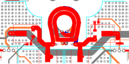
Planar Inductor

A planar converter may exist on the outer only or through-hole layers and may have a physical body applied to the outer layers. However, part of the footprint consists of copper spirals which are connected by a component via, effectively joining the two footprint pads. By defining the footprint as embedded, the Component can be mirrored in situ and all the inner layers will swap as required. Special DRC properties also allow the checking of correct internal connectivity made on the elements of these components.

Chip-On-Board Technology

Chip-On-Board

Chip-On-Board

The Chip-On-Board option provides features for creation and annotation of die & bond pads and bond wires. It also allows automatic placing bond pads around the die. Within the Pulsonix design the bond pads are treated as special pads and can move independently of die and normal pads.

Advanced Rule Sets

Chip-On-Board DRC Checks

Pulsonix contains a set of rules that are obeyed using both the Online DRC and batch DRC processes. Rules can be set for min and max length of the bond pad from the die pad, and for the crossing over of bond wires. Conditional Spacing rules can be defined for COB devices that use smaller values for this type of detailing. This is also a highly desirable requirement where mixed conventional and bare die technologies are used.

Component Interaction

Chip-On-Board

Components which contain die and bond pads are handled intelligently using an advanced rule set. Bond pads can be interactively moved independently of the main die 'body'. This movement is controlled using the min and max length rules of the bond wire, with cross-over rules also maintained in this process. The chip die can also be moved independently of the bond pads and position reset if needed.

Data Migration

Pulsonix delivers the largest collection of free Import Filters available in the industry. Import Schematic and PCB Designs as well as the Libraries from your current system; retain your Intellectual Property with accuracy and precision.

And where an import filter for your product is not available, please contact us to discuss other options, such as rebuilding your designs from Gerber data and reverse engineering the PCB back into a working Schematic design to match!

vendor logos

Discover why thousands of companies around the world choose Pulsonix

"Pulsonix has provided us with maximum value through advanced software that is used in the engineering design department."

Andreas Sauer - Hoffmann+Krippner

Request a Free Trial

All the features of the full edition and only limited to 100 component pins.

Request Pulsonix for Free

Contact Us

We have sales channels throughout the world that will be able to help you.

Contact Us