| Author |
 Topic Topic  |
|
|
marco.ruggeri
Italy
67 Posts |
 Posted - 17 Dec 2014 : 08:18:46 Posted - 17 Dec 2014 : 08:18:46


|
I need to define a custom Paste Mask shape for thermal pad of QFN footprint. Shape needs to be similar to which defined on page 5 of the following document by TI:
http://www.ti.com/lit/an/sloa122/sloa122.pdf
Please suggest how to obtain this result.
|
|
|
steve
United Kingdom
316 Posts |
Posted - 17 Dec 2014 : 09:19:06
|
The form required for the belly pad stencil windows can simply be drawn on to the Paste Layer in the footprint over the copper belly pad area. Draw this in Shape.
Pulsonix Assistance |
 |
|
|
marco.ruggeri
Italy
67 Posts |
Posted - 17 Dec 2014 : 10:20:25
|
| I added custom defined shapes on layer Paste Mask Top corresponding to thermal pad but the problem is that a paste mask is already associated to the square pad, so I obtain my custom shapes overlaying default shape…and it‘s a problem: I can I solve this ? (I tried to upload the file of the footprint but it seems that there is an error during upload … can you give me your email address?) |
|
|
|
jameshead
United Kingdom
127 Posts |
Posted - 17 Dec 2014 : 10:28:42
|
The way to do this is to create a new pad style for the thermal tab, then use BY LAYER to make the existing solder paste zero size. You need to do this on both Solder Paste layers, paste mask top and paste mask bottom.
Then you add your required solder paste apertures using Insert Doc Symbol to draw the rectangles.
I use the PCB Libraries Footprint Expert that takes care of the solder paste stencil design automatically although you still have to manually turn the solder paste off using BY LAYER for the thermal tab.
However having said this, you may find that your PCB Assembler or stencil manufacturer have their own recomendations that differ from that provided by Texas Instruments. I usually output the solder paste apertures at the same size as the normal copper pad and give instructions to the PCB Assembler and Stencil fabricator telling them to adjust the sizes to suit their own processes. |
|
|
|
steve
United Kingdom
316 Posts |
Posted - 17 Dec 2014 : 10:54:08
|
My suggestion was to apply the paste windows over the top of copper forming the belly pad area, not a pad with pad number, so there would be no other paste form auto-created. The support address is support@pulsonix.com.
quote:
Originally posted by marco.ruggeri
I added custom defined shapes on layer Paste Mask Top corresponding to thermal pad but the problem is that a paste mask is already associated to the square pad, so I obtain my custom shapes overlaying default shape…and it‘s a problem: I can I solve this ? (I tried to upload the file of the footprint but it seems that there is an error during upload … can you give me your email address?)
Pulsonix Assistance |
|
|
|
marco.ruggeri
Italy
67 Posts |
Posted - 17 Dec 2014 : 11:04:19
|
| I found the suggestion of James Head very useful and it seems to work great! In the other case (if i well undestand what you told me) if i define a belly pad as copper instead of a pad it is a little bit tricky to manage because i need to add it to a net in PCB design but i can't see this pad in the schematic and it can create confusion if schematic designer and PCB designer are not the same person. |
|
|
|
steve
United Kingdom
316 Posts |
Posted - 17 Dec 2014 : 11:46:53
|
Indeed it depends on if you need the belly pad to be a pad with pin number, in many cases there is no need to represent it in the schematic as it is there purely to evacuate heat and carries no 'in circuit' use. It can be assigned to a 'convenient' net in the PCB if of benefit.
Pulsonix Assistance |
|
|
|
Chris
Netherlands
40 Posts |
Posted - 24 Nov 2017 : 15:26:27
|
"Then you add your required solder paste apertures using Insert Doc Symbol to draw the rectangles"
I am in the footprint editor and want to ad 4 stencil openings to a pad following the above procedure.... but where can i find -> Insert Doc Symbol ?
and are the stencil openings after doing the above procedure associated to the pad ? |
|
|
|
steve
United Kingdom
316 Posts |
Posted - 24 Nov 2017 : 15:30:59
|
You add Shape (Insert Shape) making sure the shape is 'closed' and filled, on to that layer.
Pulsonix Assistance |
|
|
|
Chris
Netherlands
40 Posts |
Posted - 25 Nov 2017 : 11:27:07
|
When i am in the footprint editor it is truth that i can draw a filled rectangle on the paste mask layer above a pad, but if i move the pad the filled rectangle stays where it is drawn and that not what i want. I want a pad with four stencil openings and if i copy, move or save that pad the stencil openings must come with it. It's still not clear for me how to do that.
I have tried to define a pad shape with four stencil openings but when i try to save that pad i get the message : Padstyle has more then one shape on the layer paste mask top.
Maybe some on knows a solution. |
|
|
|
bkamen
USA
49 Posts |
Posted - 25 Nov 2017 : 16:01:27
|
Hi there,
Yes -- when you're editing the footprint, you go to the pad styles in the technology menu.
Then select the pad and then "edit by layer" and add the layer you want to be different. In this case "paste mask" for the layer you want.
(if it's SMT, use "Past Mask (Top)" in the editor. It transfers to bottom with rest of footprint if you put the component on the bottom.)
if you're doing free-hand editing on the PCB and want to add copper with solder mask relief, you can "group" the two items together and then make "tight group" and then they move as a group. You DO NOT want this for footprints -- that gets messy.
Cheers,
-Ben |
|
|
|
Chris
Netherlands
40 Posts |
Posted - 25 Nov 2017 : 20:03:52
|
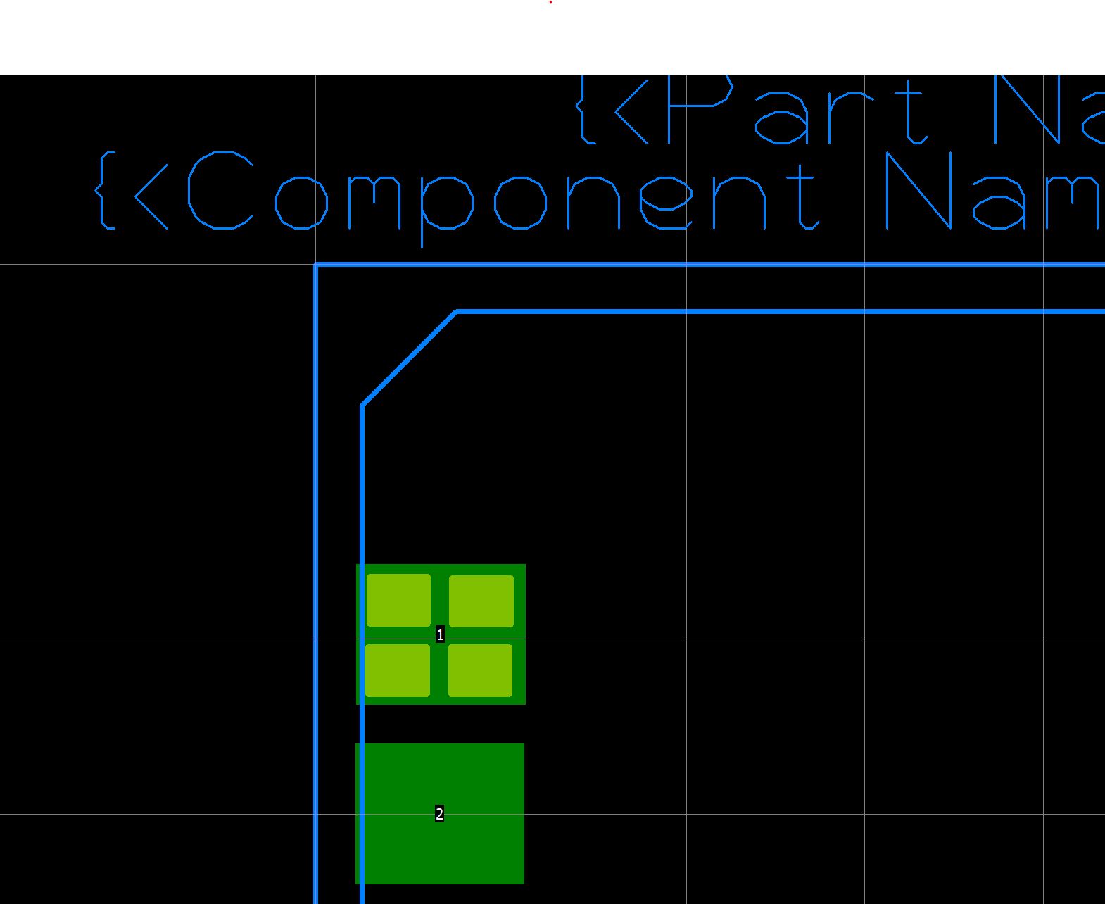
Thanks for the answer but i don't think it is what i hoped for. I know i can go to technology and use the by layer option if i want different dimension for the past mask but with that i don't get what i want.
I want four (4 !!!) stencil openings for each pad i use to make my foot print. The footprint has a lot of pads. Eacht pad must have the 4 stencil openings. So i want i pad that i can copy or save or move and while doing that the four (4) stencil openings must stay attached to the pad.
How do i make a pad with 4 stencil openings attached to it which i can save and reuse later ?
Attached a picture in which can be seen what i want. I made the 4 light green stencil openings on the paste mask layer bij drawing filled rectangles, but the are in no way attached to the pad (which is what i want). If i move the pad the stencil openings stay where they are.
Image Insert:
110.57 KB |
|
|
|
steve
United Kingdom
316 Posts |
Posted - 27 Nov 2017 : 10:19:07
|
To re-cap on some points made and to clarify others:
1. The pad style is driven from the Technology - Pad Styles. How such items as Solder Resist and Paste mask appear for pads is driven from Technology - Layer Class. However, if you modify the pad style by changing the singular pad form for a resist/paste layer then that overrides the layer class result for that layer created by the system.
2. Make sure you are managing Technology files and their use so to ensure layers are present where needed.
3. If you require a form such as these four paste windows, the 'system' created result has to be suppressed by using the By Layer and reducing the size to zero, then draw the required form, over the pad, on that layer, in the footprint. It is advised that the pad style is specific for this purpose. This would have be done for each pad position. Custom Pads (special pad style) would work the same.
4. Pad Style layer overrides will only transfer to the bottom layer with the rest of the footprint if the 'Mirror with Component' option is on in Design Settings - General for a design. Make sure any By Layer suppression is also on for those bottom layers within the pad style.
5. Pad Style overrides cannot be retained on a pad style at present. There is a log asking to allow multiple shapes per layer on a custom pad, log 29934, I have added this to that log.
6. There is a process where you could create a custom pad with multiple windows in it, to be processed for say a Resist gerber output, but this would mean a Resist layer and Layer Class per window, combined at Output. As always, Technology will need to be managed.
Pulsonix Assistance |
|
|
|
Chris
Netherlands
40 Posts |
Posted - 27 Nov 2017 : 11:19:29
|
| Ok, thanks for the clear description ! I will do it in this way. Hope in the future i can also do it also with in the user pad defenition. |
|
|
| |
Topic |
|