| Author |
 Topic Topic  |
|
|
kunalagon
Yugoslavia
15 Posts |
 Posted - 21 Nov 2014 : 09:37:39 Posted - 21 Nov 2014 : 09:37:39


|
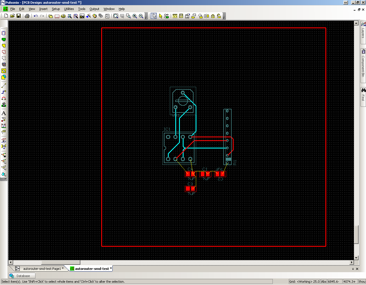
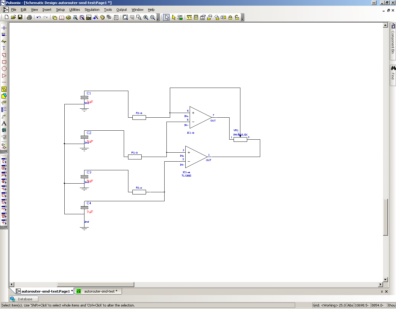
Hello,
It seems Pulsonix autorouter does not work with smd compoenents (or smd mixed with throu hole).
It just wont route many networks (in version 8.0.5536, 8.0.5544, while in version 7.6 it works flawlesly, but I cannot open files made by 8.0 with 7.6)
Here is some very simple random circuit example:
Download Attachment:  autorouter-smd-test.pcb autorouter-smd-test.pcb
39.35 KB
Download Attachment: autorouter-smd-test.sch
41.92 KB
and here is a pictures:
Image Insert:
49.72 KB
Image Insert:
36.9 KB
Now, I am wondering if I should set something in Pulsonix or this is just a bug. |
|
|
leon_heller
17 Posts |
Posted - 21 Nov 2014 : 15:15:35
|
It won't route manually, either!
There seems to be something wrong with your layers - the area lines are on the same layer as the pads and prevent the tracks extending beyond them. When I removed them the autorouter worked OK.
I used version 8.0 build 5544.
Earlier versions won't load designs made with later versions.
Leon Heller |
Edited by - leon_heller on 21 Nov 2014 15:52:26 |
 |
|
|
kunalagon
Yugoslavia
15 Posts |
Posted - 21 Nov 2014 : 15:53:26
|
This is good to know, but what should I do, do I have to edit every smd component in libraries or what?
This was normaly working with version 7.6
I think Pulsonix should know diference between pads and component border.
Thank you. |
Edited by - kunalagon on 21 Nov 2014 16:17:48 |
|
|
|
steve
United Kingdom
316 Posts |
Posted - 21 Nov 2014 : 16:27:18
|
Hello..
The problem is not layers. The problem is your surface mount footprints. The area surrounding the pads is set to keep out both tracks and via's. If you manual routed to them with On-line DRC on set to Continuous then it would not allow entry to the area.
Modify your footprint to allow routing in.
Pulsonix Assistance |
|
|
|
steve
United Kingdom
316 Posts |
Posted - 21 Nov 2014 : 16:30:00
|
Oh and the area is on the right layer, the same layer as the SMT pads. Also you are right, designs will not read back into an earlier version of the product.
Pulsonix Assistance |
|
|
|
leon_heller
17 Posts |
Posted - 21 Nov 2014 : 16:38:10
|
Yes, that's it. He has tracks and vias set to Keep Out. My parts have the tracks and vias set to Unrestricted in the Area Properties.
Leon Heller |
Edited by - leon_heller on 21 Nov 2014 16:42:15 |
|
|
|
kunalagon
Yugoslavia
15 Posts |
Posted - 21 Nov 2014 : 16:49:21
|
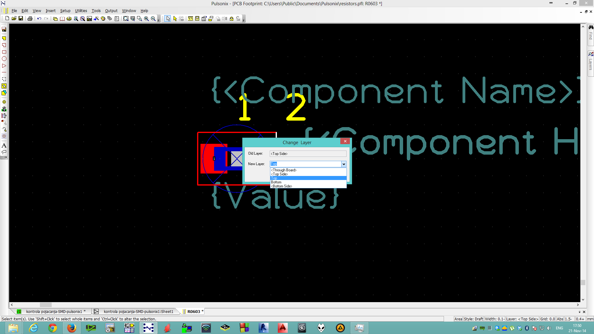
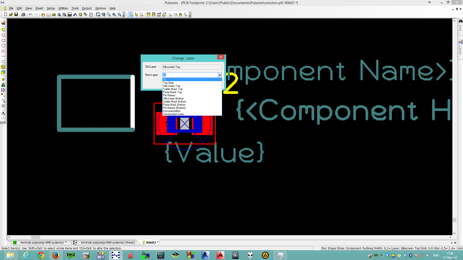
Yes, you are right. I set to unrestricted and now it works.
But, what layer type is you rectangular poligon? I am not able to set anything but top and bottom layer, and I want to set that poligon area to silkscreen like other componets are set to. And when I make another poligon using rectangular poligon tool it is able to choose between many layers
here is a pic:
Image Insert:
90.01 KB
Image Insert:
91.37 KB
|
Edited by - kunalagon on 21 Nov 2014 16:50:59 |
|
|
|
leon_heller
17 Posts |
Posted - 21 Nov 2014 : 17:05:09
|
You should add it to the footprint on the Silkscreen Top layer.
Leon Heller |
Edited by - leon_heller on 21 Nov 2014 17:09:42 |
|
|
|
steve
United Kingdom
316 Posts |
Posted - 21 Nov 2014 : 17:21:12
|
For a SMT device, I would recommend Areas being set to, in most cases, <Top Side>. Although the other choices on the drop-down can be useful for particular circumstances.
Shape does not carry active properties so is used on layers such as silkscreen, assembly, documentation and can be used in certain circumstances to add to paste and resist layers.
Pulsonix Assistance |
|
|
|
kunalagon
Yugoslavia
15 Posts |
Posted - 24 Nov 2014 : 09:08:10
|
I still cant change layer from TOP SIDE to some sort of SILK/DOCUMENTATION layer, because, as we can see on screenshot, drop down menu does not offer other layers.
Those footprints are from eaglecad libraries.
For now, solution is to change that layer to unrestricted.
It seem the problem is in EagleULP scripts, script does not recognize eagles layers 39(tKeepout) and 40(bKeepout) and convert it to TOP SIDE insteed to silkscreen or some documentation layer. |
|
|
|
steve
United Kingdom
316 Posts |
Posted - 24 Nov 2014 : 11:36:25
|
Please supply the resultant eagle footprint library file (.eil) after running the ULP to support@pulsonix.com
Pulsonix Assistance |
|
|
| |
Topic |
|