

The Define Pad Shapes option allows you to define your own pad shape which is not one of the standard shapes available.
One created, these special pad shapes can be saved into a PCB Documentation Symbol library. The pad shape in the library contains all shapes, construction lines, text, dimensions and text callouts, the pad style in a PCB design only contains the shapes.
Shortcuts
Default Keys: None
Default Menu: Setup
Command: Define Pad Shape
Locating this option
Available from: Setup menu > Define Pad Shape option
Available from: Setup menu > Technology dialog > Pad Styles page
Define Pad Shape option
How to Define a Pad Shape
The are a number of ways that you might create your own pad shape. The Define Pad Shape editor option will be used from any of these entry points:
- You can create a special Pad Style in the Technology dialog (from a PCB design or within the Footprint editor). Create a new style or preferably modify an existing one that is of a similar starting shape you wish to define. Use the Define New Pad Shape button to create/modify the new shape. Or* From within your PCB design, select an existing pad shape and then from the Setup menu, select Define Pad Shape. This will modify the existing Pad Style once save is pressed, all pads in the design using that style will be changed. If you want a custom pad style for just one pad instance, create a new Pad Style for use. Or* From within the Library Manager with a PCB Documentation Symbol Library open. Use the New button to add a new documentation symbol of type Pad Shape.
Define Pad Shape Dialog
When accessing this option from the Setup menu with no existing pad style selected, you are presented with the Define New Pad Shape dialog.
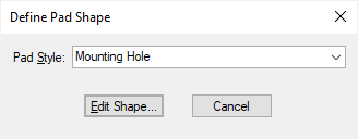
Select an existing Pad Style from the drop down list or type a new name of the Pad Style you require. Press the Edit Shape button to open the Define Pad Shape Editor.
The Pad Shape Editor
To create and modify a special pad shape, Pulsonix has a Pad Shape Editor.
With an existing pad selected, the original Pad Style shape is presented as a starting point for you to edit. If starting by typing your own name and using the Edit Shape option, the view will display a pad Origin and a basic built in pad shape of a Square pad style with a Drill hole. It is easier to start with an existing shape as it sets up the layers and default shapes for you.
The diagram below illustrates the shape outlines presented along with their colour coding. Each pad shape entity within this editor has a colour to aid identification, these are taken from the current design, or from the Technology file if editing a pad shape symbol from the library.
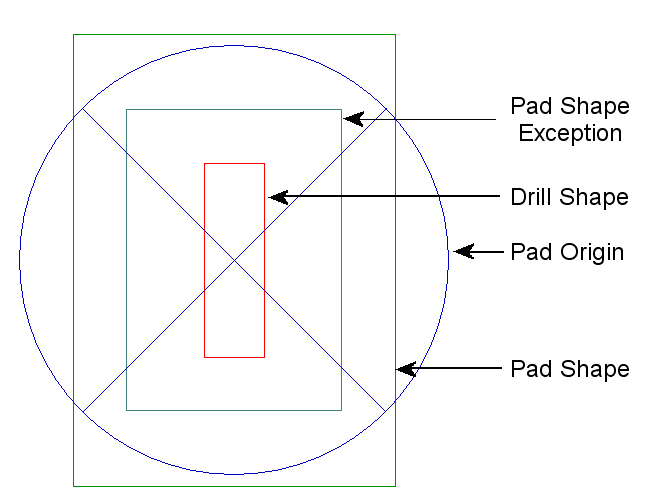
Pad Entities
Shapes
The shape will be on a special layer called <Default Shape>.If you already have Pad Exceptions on other layers, they will also be present on the appropriate layers. You can use the Merge Shapes command to create a composite shape for more complex pad shapes required.
During editing, you can edit or create new shapes on any of the layers and also delete existing shapes. You can also create several shapes, but at the point it is saved, only a single shape (or no shape) should be left on each layer. The exception is Non-Electrical layers, which can have several shapes defined on them.
A shape that represents the pad shape on all inner layers of the board is created by placing the shape on the special <Inner Electrical Shape> layer. Only one of these pad shapes should be defined and this is checked when you attempt to save the pad style.
A shape on all layers of a layer class is defined by first adding the shape on a layer using the required layer class, and then marking it using the Toggle as Layer Class Shape context menu option. There should be only one of these shapes on each layer class as it represents the pad shape on any layer using the class. This will be checked when you attempt to save the pad style.
A Spacing Shape is defined by marking it using the Toggle as Spacing Shape context menu option. Spacing Shapes should only be defined on an Electrical layer or the through hole layer and there should be only upto one shape on each layer. This will be checked when you attempt to save the pad style.
Drill Hole
If the Pad Style has a drill defined, this is also shown as a shape on a special <Drill Shape> layer, you can use the editor to move or edit the drill. The shape on the drill layer can be any shape, so you can create a slotted pad. An origin symbol shows where the origin of the shape is, this is normally the connect and drill point (but it can be offset).
Micro-vias
Micro-via Entry and Stop Pads are defined by placing the shape on the special <Micro-via Entry Pad> or < Micro-via Stop Pad> layers. Only one Entry and Stop pad shape should be defined and this is checked when you attempt to save the pad style.
Origin
Place the pad Origin where required. This can be the centre of the pad or at an offset within it.
Saving the Pad Style
Once you have defined the shapes, use the Save option to save it back into the Pad Style, or to save it back to the library if editing a library symbol (this is optional and is only used if you wish to create a library of special pads shapes).
When the pad style is saved, the program will attempt to identify standard predefined shapes, such as Circle, Square, Rectangle etc., and use this type. If it can identify a standard shape, it will create user-defined Special shapes for the other pad shapes. Predefined shapes can still be modified using the Pad Style Edit dialog, whilst Special shapes would need to be edited using the Define Pad Shape option again.
Loading Partial Technology Files and Special Pad Styles
If you save Special pad shapes into the design Technology or into a Technology file, you can partially load just these pad shapes using the Load Technology File option and selecting the Pad Styles required.
Save To Library
As well as using Save to save and exit the Pad Shape Editor, you can also use the Save To Library option. This will save it to a special type of documentation symbol into a PCB documentation symbol library for use in other designs.
Using this option allows you to include elements such as text, dimensions and callouts to the pad shape definition, making it easier to refer back to and modify at a later date.
Load Pad Shape From Library
When editing a pad shape from a design or Technology file you can use Load Pad Shape From Library from the context menu to replace the pad shape being edited with the contents of a symbol from a PCB documentation symbol library or vault.