

Use this when editing a Part to define the Part as a Bus Register.
Use this on a Bus Register component in a schematic design to change its parameters, or to replace it with a Bus Register part using a different number of bits or output enabled state.
These parts are implemented by using Functional Modelling. They have their Spice Type Built-in Function set to Bus Register.
Shortcuts
Default Keys: F7
Default Menu: Simulation
Command: Edit Spice Value/Model
How To Add A Bus Register
There are various ways to add a Bus Register to a Schematic Design:
- From the Parts toolbar, click on the Digital Generic pop-up to display the Digital Generic toolbar. Click on the Bus Register button.
- From the Parts Browser, click on Spice Category, then on Digital and Generic to display the Digital Generic parts. Drag the Bus Register part name into the design. Note: This method may not work if you have changed the part categories.
- Use Component from the Insert menu to add the Part called Bus Register from the Spice library.
Whichever method is used, you should be presented with the Define Bus Register Dialog described below. This works because the part named “Bus Register” has a blank function definition which forces the dialog to be given to get the required definition from you.
How To Define A Bus Register
In a Schematic Design, select the Bus Register device(s) that you wish to change. Press F7 or use the Edit Spice Value/Model option from the Simulation menu, or from the shortcut menu.
From a Parts Library edit the required Part. Press the Edit Spice button on the Details tab. Make sure the Built-in Function is set to Bus Register and press the Edit Definition button.
In both cases the following dialog will be displayed:
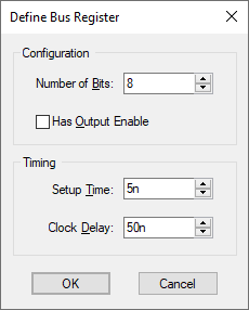
Number Of Bits
Enter the width of the register. Valid values are from 1 to 32.
Has Output Enable
Check this box if the register output should control the output enable.
Setup Time
Enter the setup time in seconds. This is the time that the input data must remain stable after the clock edge, for the new value to be accepted.
Clock Delay
Enter the register delay in seconds. This is the delay between the clock rising edge and the register value changing.
See the Arbitrary logic block section in the Simulator’s Device Reference Manual for more details.
Changing the Symbol
If editing a Part, make sure the chosen Number Of Bits and Output Enable state match the Symbol that is used by the Part.
If editing a component in a schematic design, pressing OK with changed Number Of Bits or Output Enable state will force the component to be replaced with a Part from the Library that matches the new specification. If no suitable Part exists, an error message will be given giving details of the Part that will need to be created.
Editing Multiple Components
If any of the fields are set to <Different> then some of the components you are changing have different values for that field. Clear this field and enter the required value for all components, or leave as <Different> to tell components to keep their original values for that field.