This page gives more detailed information about the Auto Rename options.
Note that some of the functionality described below is only applicable when using Auto-Rename for a PCB design and not when used for a schematic design.
Channel Width
The Channel Width value provides you with a method of dividing the width of the board into ‘channels’ so that the rename option knows where to find the names when making the renames.

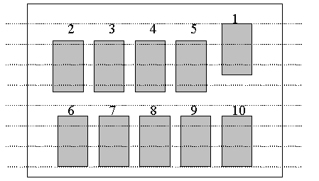
When considering the channel width you should be aware that the channel will look at the centre of the component bounding box including the component silk screen information but excluding the component name.
The width to be used will depend on the type of components on the design, for fine pitched devices a lower value should be used but if conventional components have been used then make it larger. Typical values might be 100 thou, for an SMT design with mixed technologies, or 250 thou for a conventional through hole design.
Care should be taken defining the Channel Width, if you get renames which are unexpected or the sequence appears out of step, the channel width should be checked. Components will be renamed in a channel if their centres are in the channel ‘band’ as the example above shows.
Components
Use this to input the component name stem used for the rename. If ‘U’ is selected for example, all the components starting with the letter ‘U’ followed by a number will be renamed, the same if ‘R’ or ‘C’ etc. are selected in turn for rename. This is only used if the check box for Selected Stem Only is selected otherwise all items of like stem name will be renamed.
Rename Direction
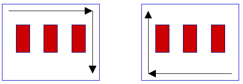
Use this to select the direction of the renames whether it is biased side to side or top to bottom.

The selection for the rename directions are Left to Right or Right to Left, or Top to Bottom or Bottom to Top. Once the first direction has been selected, the From entry will only allow the opposite bias to be selected, e.g. you cannot select Left to Right and then Right to Left in the From box, the directions must be X followed by Y or Y followed by X. It is normal practice to direct the renames to be left to right followed by top to bottom. This practice means any service engineer can pick up a PCB and find a component quickly just by looking at it knowing that a name convention has been used.
Location
If the rename By Location check box is not selected all renames will be done in consecutive order, if this is checked the rename will be done using the Direction and Side specified, and the Channel Width.
Reverse
This can be used when either the Both or Bottom side are selected for Side. The effect is that the name direction on the back of the finished PCB will still be readable when Left to Right is specified as the horizontal direction.
Side
The selection in the Side list box gives the opportunity to select Top Side, Bottom Side or Both Sides. If Top or Bottom Side are selected the rename is only performed on that side. If the Both Sides selection is made the rename will rename one side first followed by the other side, using the direction specified. The direction does not change when renaming the ‘back’ of the design, so effectively the renames on the back are the opposite direction when to the direction chose when viewed from the other side of the board. If you require them to be the correct readable direction when viewed from the bottom of the board, select the Reverse Direction check box.
Rename Type
Automatic renames can be used on Components, Testpoints and Net names. For Components and Testpoints all names will be made consecutive using the component or testpoint stem name (e.g. U or TP would be used). For nets all net names are made consecutive and all name ‘gaps’ removed.