Insert Bond Pad is used to when creating a footprint for a bare die component. It is used to insert and place a bond pad which will be attached to a selected die pad by a bond wire.
Unlike die pads and normal pads, bond pads are usually individually positioned after the component containing them has been added to the PCB design. If a bond pad in a PCB design cannot be moved, make sure it has its Allow Interactive Reposition property enabled.
Shortcuts
Default Keys: None
Default Menu: Insert
Command: Insert Bond Pad
Locating this option
Available from: Insert menu > Insert Bond Pad option
How To Insert A Bond Pad
-
Select the Insert Bond Pad icon from the Insert Toolbar, or from the Insert menu, select Pad.
-
Left click on the die pad that you wish to attach the bond pad to.
-
A bond pad will appear in the footprint (moving at the end of the cursor), attached to the die pad by a bond wire. If another bond pad was selected prior to entering the option, then the new pad’s style and layer will be copied from it. Otherwise, the pad’s details will be as defined in Bond Pad Defaults.
-
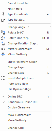
Right click to use the shortcut menu as follows:
 * Rotate - the pad (if it has a length) to the correct orientation.
* Auto Rotate - Use to keep the pad's orientation relative to the angle of the
attached wire.
* Mirror - the pad's shape.
* [Change Style](../Change/idh_change_style_pad.md) - to use a
different shape
* [Change Layer](../Change/idh_change_layer.md) - to make the
pad through hole or surface mount.
* [Online DRC](../Options/idh_options_online_drc.md) - to restrict positioning
of the pad to conform with the design rules settings within the Technology data.
* [Display Clearance](../options/idh_display_clearances.md) - to
present a visible warning if you are positioning a pad too close to another
item within the design.
* [Change Grid](../Change/idh_change_grid.md) - To change the
grid step, or work with no grid.
-
Move the bond pad to the correct position and left click to release it. Then click on the next die pad to wire to a bond pad.
-
When all bond pads have been added, press the Escape key to exit the insert bond pad mode.
Editing Bond Pads in a PCB Design
Bond pads can be individually moved and rotated after the component containing them has been added to the PCB design. If they cannot be moved, make sure they have their Allow Interactive Reposition property enabled. You can also use the Select All Bond Pads option from the shortcut menu when part of a single component that contains bond pads is selected in a PCB design. Use it to select all the bond pads on the component. Alternatively, if you have already placed the bond pads in their correct locations, use the Move Chip Body option from the shortcut menu to move the chip body without moving any of its bond pads.
Using Change Layer, you can set the layer of an individual bond pad in a PCB design to any reference layer that is facing the same way as the layer the component is on. This is to allow the placing of the body of bare die components into cavities and have their bond pads still on the top side. You can also change the layer of multiple bond pads on one component using the Properties dialog.
Related Topics
Change Grid | Change Layer | Change Style | Display Clearance | Insert Die Pad | Online DRC | Pad Defaults | Technology