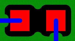
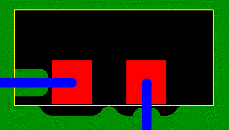
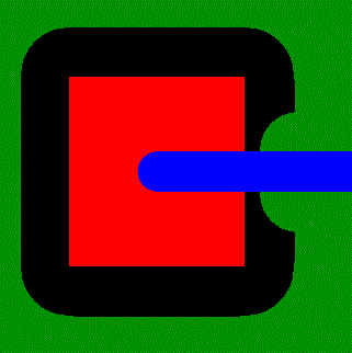
The Anti Pad Rules dialog is used to specify the rules used to generate additional copper plane cutouts on layers below pads (or vias, mounting holes, etc). When copper is poured, or a Power Plane generated, these cutouts are applied.
The general rule matching mechanism is described here.
Shortcuts
Menu: Setup
Default Keys: T
Command: Technology
Locating this option
Available from: Setup menu > Technology option > Rules - DFM/DFT - Anti Pad page
Using the dialog
On selection, the Technology dialog opens, select Adjacent Nets Rules. The existing Anti Pad Rules for the Technology being used will be presented.

Navigation
The buttons to the right side of the dialog are used to navigate the grid, the general common buttons are detailed on the Technology Navigation page.
Using the editing pane

A rule defines the pads (vias or mounting holes) which will generate cutouts. The order of the rules is significant, the first matching rule is applied.
Attribute Name & Match Value
A match is when the specified Attribute Name and Match Value match attributes of a net or pad. So
the pad (or net) must have the given attribute, and it’s value must
wildcard match the value. In particular, you can match the inbuilt
attributes
On Layer: Side, Layer & Area
You can also restrict the rule to apply only to pads on the specified Side or Layer; or within the matching named area.
Applies To
You can make the rule specific to a type of pad (Any, Through Hole Pad (including Through Mounting Hole), Surface Mount Pad (including Surface Mounting Hole), Via (including Micro-via), Micro-via, Through Mounting Hole, Through Mounting Hole). Select the appropriate type in the list.
Note that the first matching rule will apply, so you need to define the rules in the correct order (e.g. a Micro-via rule should come before a Via rule).
Shape
Define the parameters of the anti pad shape.
Pad To Plane
Define the oversize to be applied to the pad shape. You can blank out this field to

Merge Pad Distance
Merge pad shapes within this distance. This gives an ‘oval’ around a pair of pads, or perhaps a pair of vias on a
differential pair. You can blank out this field
to

Include Component Body
This option will generate a cutout around the whole component body of a matching pad.

Adjacent Layers
Use this option to specify how many adjacent layers away from the pad layer this rule applies on. So for a pad on
the top (layer 1), and adjacent layers set to 1, a cutout is only generated for a plane on the adjacent layer
(layer 2), and not on any subsequent layers. (0 or
Nub In
A Nub In is an indentation into the cutout generated underneath a track entering the pad.

Track to Plane Edge
The amount the track width is enlarged. You can blank out this field to
Pad to Plane
How much to back off the Nub In shape from the pad.
Adjacent Layers
Put the Nub In shape only on the number of adjacent layers (even if the main shape is on a greater number or all
layers). (0 or
Export and Import CSV
Use the Export CSV button to export the data in your PCB design into a CSV format file. Using the Export CSV option will provide you with a formatted template ready for you to edit in your own data.
Use the Import CSV button to import the data back in your PCB design.
The data in the file represents a spreadsheet of dialog contents with the data headings along the top row.
Units
The Units button allows you to locally switch between Metric and Imperial units whilst in this dialog. Once the dialog is closed, the units revert back to the original design units. If switching to different units to the design units, the value typed will be converted when you next enter this page.
Related Topics
Technology Overview | Using Dialog Grids | Net Name | Layers | Areas | Technology Rules | Wildcard Matches | Design Rules Checking | Options - Warnings | Net DRC Errors Bar | Colours - Text Warnings Export CSV | Import CSV