The Panel Wizard is used to start a new Panel for multiple copies of a particular PCB design. It allows you to set up basic parameters about the panel such as the Technology used, Panel Profile, Units, overall panel size and the ‘array’ pattern for the PCB instances on the panel. The Preview panel displays the panel contents as they are changed in the wizard.
Shortcuts
Default Keys: None
Default Menu: File
Command: Panel Wizard
Locating this option
Available from: File menu > New option > Wizards tab. It is also available as an icon on the standard toolbar, next to the other wizard icons.
Using this Wizard
The Panel Wizard breaks down the process of creating a new Panel into a series of steps. Each step is presented in turn on a separate wizard page. Complete each step then move onto the next one until you reach the Finish page. At any time as you progress, the preview window will give you an idea of what your final panel will look like.
Start Page
The Start page of the Panel Wizard is your initial page when the wizard is initiated.
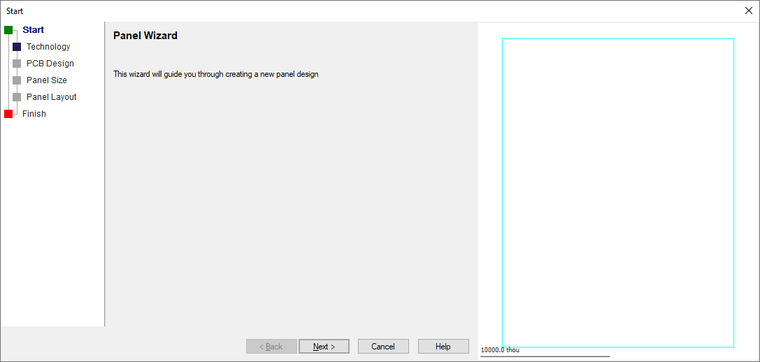
The preview shown at this stage shows the panel with the options you chose last time you used the wizard. Additional data for the panel such as tabs, V-Scores, test coupons etc. are added interactively through the panel editor after the panel has been created by this process.
Technology Page
The Technology page allows you to specify your technology requirements for defining your panel. As with the rest of the application, the Panel Wizard utilises Technology Files as a means of applying a consistent set of CAM/Plots, styles, rules and constraints to the design process. The Panel Wizard uses the same type of Technology file as your PCB design.
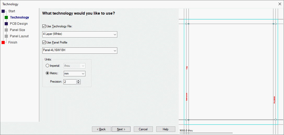
If you check the Use Technology File box, the PCB design you will add to the panel later in the wizard process will have to match the electrical layers and layer spans in the technology file you select from the drop down list. If you choose not to use a technology file, the technology section of the resultant panel design will be taken from the PCB design, including all CAM Plots, Layers and Variants.
Check the Use Panel Profile box if you have previously created a suitable Panel Profile design containing the correct outline shape and size, and maybe some panel furniture (e.g. tooling holes, Fiducial markers, copper bars). Pick the file from the drop down list. You will see the outline displayed in the preview.
You should also choose the Units to use to define this panel. These will be the units used in subsequent steps. Obviously the most important choice is between Imperial and Metric units. They will be initialised to the units in the chosen technology file.
PCB Design Page
This page allows you to choose the PCB design to insert into the panel.
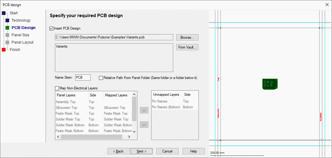
To add a PCB design to the panel, check the Insert PCB Design box and use the Browse button to locate your design. If you are using a specific technology file and the chosen PCB design does not match the electrical layers and layer spans, an error message will be shown and the PCB design will not be selected. The full path of the selected PCB file will be shown in the file name box, and the box below will display the description of the PCB design, extracted from the Comments field in the Summary section of the PCB designs document properties.
You can choose to leave the panel empty by unchecking the Insert PCB Design box. PCB Designs can be added interactively using the Panel Editor later on. At that stage, you can also add multiple PCB Designs of the same type or different designs.
Relative Path From Panel Folder: There are two ways of locating the PCB design file in the future when the panel design needs to access its data, for example when generating plots. The first way is to use its absolute file location. The second way is to access it in the same folder as the panel design, or in a folder below the panel design. Do this by checking the Relative Path From Panel Folder box. This is useful when saving the panel design with the PCB design, because if they are both then moved to a different folder the panel will still be able to find the design.
Name Stem: is used to define the local name for the PCB instances within the panel. A number will be added to the name for each instance to uniquely identify it.
If you are using a specific technology file for the panel, the non-electrical layers in the PCB design may not exactly have the same names as the layers in the technology. In this case, check the Map Non-Electrical Layers box to map the names.
Select the PCB layer you want to map in the Unmapped Layers column, then select the panel layer you want to map to in the Panel Layers column and press the ”<<” button. If the sides are the same the layer name should move columns. To remove a layer name mapping select it in the Mapped Layers column and press the ”>>” button. It will move to the Unmapped Layers column. Any non-electrical layers left in the Unmapped Layers column will not be used for this PCB design when creating plots from the panel.
Uncheck the Map Non-Electrical Layers box if you do not need a mapping. If you did not choose a technology file the layers in the panel will be created from the PCB design and so do not need to be mapped. If you did use a technology file, any non-electrical layers that do not have exactly have the same name as a layer in the technology will not be used for this PCB design when creating plots from the panel.
Panel Size Page
Use this page to define the size of your panel or use a pre-defined panel size.

Define Panel Size: Use this to type the exact panel dimensions required. If you will always be using a panel of the same size, use this option as it will be remembered next time you enter the panel wizard.
Use Pre-Defined Panel Size: Choose from a list of some of the industry standard panel sizes.
**Use Outline From Chosen Panel Profile:**This option is only available if you have chosen to use a Panel Profile and it contains a panel outline. The panel outline will be copied from the profile to the panel.
Use Outline From Another Panel Design: Use this if you want to copy the panel outline from a panel design or panel profile that you have previously created. Use the Browse button to locate the panel design to take the outline from.
Panel Layout Page
Use this page to define the layout of the panel and the number of boards in the array. All values will use the units defined at the Technology stage of this process.
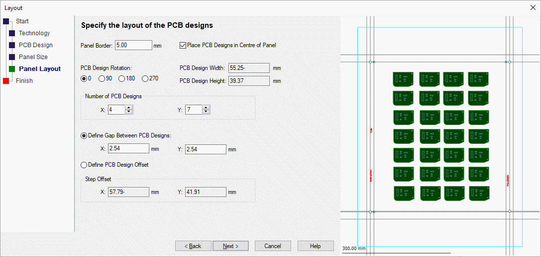
Panel Border: Define the minimum distance between the edge of the panel and each PCB board outline. This border can be used later in the Panel Editor to contain tooling holes, Fiducial markers, copper, text or other panel features. This value is extracted from the Design Rules section of the chosen technology file. The panel border value entered here will be saved in the panel design in the Design Rules section, and will be used by Design Rule Check when checking the final panel.
Place PCB Design in Centre Of Panel: Check this box to place the design in the centre of the panel. If left unchecked, the PCB design will be placed in the Bottom Left hand corner of the panel, avoiding the border. Multiple boards added will be placed from the centre ‘out’ if this check box is selected.
PCB Design Rotation: Define whether the board or boards will be rotated. Using the radio buttons, choose from 0, 90, 190 and 270 degrees of rotation. Each board is rotated individually.
PCB Design Width and PCB Design Height are non-editable fields and show the PCB design width and Height for reference.
Number of PCB Designs: Define the number of designs in the X and Y directions. The preview will be updated each time you change any values on this dialog. You simply leave this as X=1 and Y=1 if you only require one PCB to be added to the panel or if you wish to add more of a different design later on.
Define Gap Between PCB Designs: Define the gap between each board using values for the X and Y directions. If you are going to use V-Scoring to separate the boards after manufacture, use this option with a value of zero to ensure the centre lines of the board outlines are aligned.
Define PCB Designs Offset: As an alternative to the Define Gap Between PCB Designs, use this option to define specific offset values in the X and Y directions. The offset value is taken from bottom left hand side of the boards’ bounding box. In the case of circular boards, the bounding box is calculated as a rectangle around the board.
When creating the panel and adding PCB designs to it, if the boards exceed the panel outline, a warning message is displayed:

Finish Page
Once satisfied that the panel is created as required, use the Finish page to create the panel design.
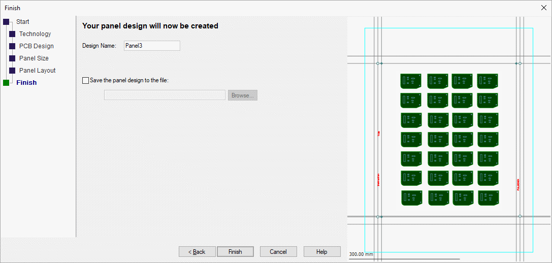
Type the Design Name of the panel. When the Finish button is pressed, the panel will open using this name in the Panel Editor. At this point the panel has not been saved; only created with a panel name.
Check the Save the panel design to the file: if you wish to save the panel to a file. Use the Browse button to choose the save location. When the Finish button is pressed, the panel is saved using the typed name and opened in the Panel Editor.
Related Topics
Panel Editor | Insert PCB Design | Insert Panel Outline | Insert Panel Tab-Rout | Insert Panel V-Score | CAM Plot