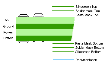
The system supports an unlimited number of Electrical, Non-Electrical and Documentation layers. These layers describe the physical ‘make-up’ of the manufactured PCB. You can define the Layers in a Technology File which can be applied to a PCB design. Each facet of the Layer is controlled using a Layer Class which is also stored in the Technology.
Locating the Layers option
Available from: Setup menu > Technology > Layers tab
Locating the Layer Class option
Available from: Setup menu > Technology > Layer Class tab
A typical or default layer configuration
Below is an illustration of a typical 4 layer PCB showing the 4 electrical layers, 2 outer layers - Top and Bottom and the inner power plane layers - Ground and Power. As well as electrical layers, you may also need non-electrical layers for additional manufacturing processes which are not constructed as physical layers but which use the electrical layers to ‘host’ their information. Typical examples for this type of layer might be; a Silkscreen layer which is printed on top of the Top Electrical layer; or a Paste Mask layer where the pad shapes are oversized to give access to the pads for soldering.
For additional information which is not a manufactured process, you may require an additional layer, this can be added as a documentation layer. This layer might contain the board build information which is used by the manufacturer to inform him how to build the board itself.
The type of layer and how and what can be shown on that layer is controlled by a Layer Class. A class can be used by more than one layer (usually a Top and a Bottom).

You can also use a more advanced layer structure where the actual construction layers are defined as well as the basic layers. Layers such as the fibreglass board (FR4) or the copper attached to it, can be defined as can their thickness and electrical characteristics.
You can also define layer stacks which support Embedded Components.
Examples of Layer Types
A Silkscreen layer will show the board outline, component outlines which are broken around pads and text. But pads themselves are not shown. This is all achieved by defining a Layer Class (called Silkscreen, with the appropriate display options set).
A Solder Mask will require breaks for all the through hole component pads so that they can be soldered. The breaks will need to be a slightly oversized version of the pad. Again can all be achieved by defining an appropriate Layer Class.
A Paste Mask layer is very similar to a Solder Mask layer in that is requires a break for each pad, but this time using a negative oversize to achieve an undersize. Again can all be achieved by defining an appropriate Layer Class.
Related Topics
Technology - Layers | Technology - Layer Class | Technology - Layer Spans | Change Layer | Change Via Layer Span | Layer Materials | Layer Drawing Order | Embedded Components