This calculator calculates the characteristic impedance of a unit length PCB track at a user provided width for a set of common track geometries.
It can also be used to calculate the track width required for a unit length PCB track to adhere to a provided characteristic impedance.
The calculator can either be used by typing the values into the dialog, or some of the values can be taken from a selected segment of track.
Shortcuts
Default Keys: None
Default Menu: Utilities
Command: Design Calculators
Locating this option
Available from: Utilities menu > Design Calculators option
Using this option
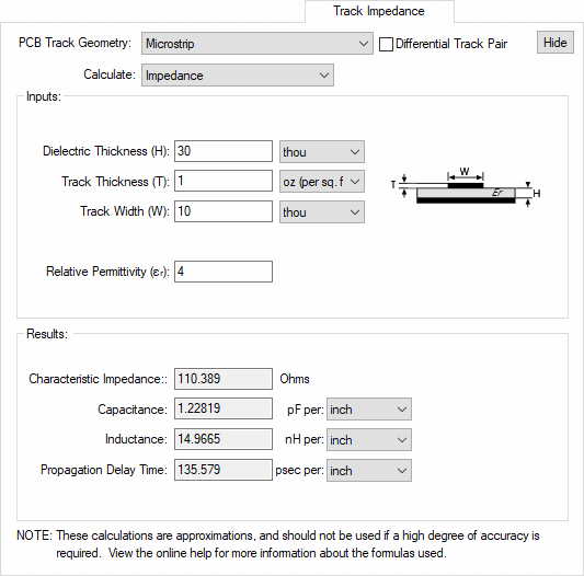
This calculator is on a tab on the Design Calculators dialog, available from the Utilities menu. The following dialog appears when the Track Impedance tab is selected.
Track Geometry
There are two controls that define the track configuration to be used in the calculations.
First drop down the PCB Track Geometry list at the top of the dialog and choose the geometry that matches your track situation.
Then use the check box to the right of the list to select whether you want the calculation for a Differential Track Pair or a single ended track.
What to Calculate
Drop down the Calculate list at the top of the dialog and choose which value you would like to calculate. The controls in the Inputs section will alter to provide the inputs for the calculation you have chosen and the Result section will display the chosen value.
Inputs
The controls in this section will be changed to match the chosen configuration and each will include a label in brackets referring to a label on the diagram.
Enter the correct values to generate the required result. Make sure the units drop down lists are correct for the values you have entered.
You can automatically enter some values in the dialog by picking on a track in the PCB design. To do this, move the cursor out of the dialog and you will be presented with a calculator cursor. Use this to pick on the track in the design and any information that can be extracted from it will be automatically entered into the dialog. Extracted values will be presented in bold text in the dialog.
If you can not see enough of the design, use the Hide button at the top right of the dialog to hide the dialog until the mouse key is clicked. In the hidden mode the calculator will work “On-The-Fly” and will present the results from the track the cursor is hovering over in a tooltip window. Click on a track, or use the “On-The-Fly” command from the context menu, to see the full dialog again.
Track Geometry
From the dialog you can choose a specific track geometry to use in the calculation, or you can choose to try and extract it from the a picked track segment. To do this move the cursor out of the dialog and right click to choose “Auto Detect Track Geometry” from the context menu. The next picked track will be analysed along with the layers either side to see which geometry it best matches.
Differential Pair Track
If a track segment is picked this check box will change to show if the picked segment is paired. The dialog will change to accommodate a paired or single ended track.
Track Width
If you are calculating the Track Impedance, you can enter the Track Width by picking on a track in the PCB design. If you use shift click to select a whole track, the largest width will be used.
Track Thickness
This will be extracted from the layer of the picked track if defined.
Dielectric Thickness
For some track geometries this is called Dielectric Below Track, Dielectric Above Track and Track To Plane Gap. In each case if a track segment is picked the layer stack will be examined to see if it can extract the thickness of the relevant Dielectric layer from its Material.
Relative Permittivity (Er)
As well as the thickness, an attempt will be made to extract the relative permittivity value from the Dielectric Constant value for Material of the relevant Dielectric layer.
Track Spacing
This is only presented for differential paired tracks and is the gap between the track pair. If a differentially paired track segment is picked the spacing between the tracks will be automatically entered into the dialog.
Conductor Space
This is only presented If you are calculating the Impedance for coplanar waveguide track geometries. If a track segment is picked that is within a template or on a power plane layer the conductor space will be set to the track to copper spacing at the picked position.
Impedance
If you are calculating the Required Track Width or Required Conductor Space, you will be presented with either the Characteristic Impedance or Differential Impedance control to enter the known value. These values will be extracted from Track Impedance Rules used by the net or differential pair of the selected track if available.
Results
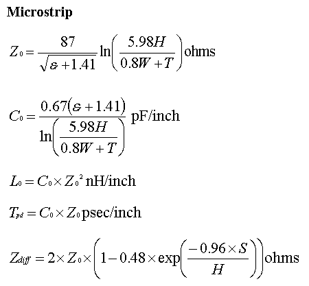
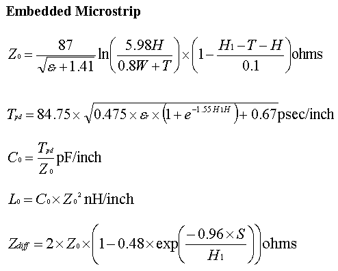
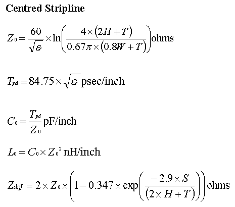
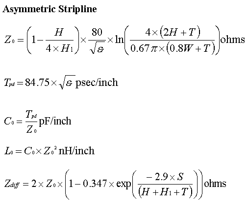
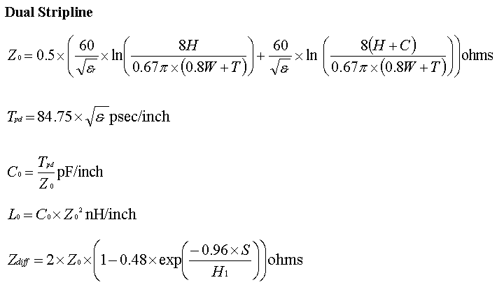
This section shows the results of the calculations using the formulas listed below. Some calculations have constrains on the relationship between parameters and, if these are not met, an error message is shown on the top line of the Results section. The message will show the relationship and state a minimum or maximum value.
Once you have calculated the Characteristic Impedance, you can switch to the Conversion Calculator tab to see the result in engineering or scientific notation.
Formulas
The formulas used are taken from “The Design Guide for Electronic Packaging Utilising High Speed Techniques” IPC-2251 document, “Transmission Line Design Handbook” by Brian Wadell, and “Coplanar Waveguide Circuits, Components, and Systems” by Rainee Simons.
NOTE: These calculations are approximations, and should not be used if a high degree of accuracy is required.









Coplanar Waveguide


Coplanar Waveguide With Ground


Edge Coupled Coplanar Waveguide With Ground


NOTE: These calculations are approximations, and should not be used if a high degree of accuracy is required.
References
“The Design Guide for Electronic Packaging Utilising High Speed Techniques” IPC-2251 document
“Transmission Line Design Handbook”, by Brian Wadell.
“Coplanar Waveguide Circuits, Components, and Systems”, by Rainee Simons.
“PCB Impedance Control: Formulas and Resources”, by Doug Brooks.
Based on the “PCB Trace Impedance Calculator” from the University of Missouri-Rolla EMC Laboratory.
Related Topics
Conversion Calculator | Heat Sink Calculator | RLCF Calculator | Scientific Calculator | Track Width Calculator | Via Resistance Calculator