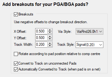
The Footprint Wizard only shows the Breakouts page when you are creating a PGA/BGA footprint.
It allows you to define a breakout pattern for the pins in the grid array.
Locating this option
Available from: Setup menu > Libraries > PCB Footprints > Wizard button
Using the Footprint Wizard
A simple breakout can be defined for each pin, which consists of a diagonal track, stubbed out to a via.

The direction of the breakout track may be changed by specifying a negative value for the X and/or Y Offset.
The Via Style will generally come from the technology file being used, but it is possible to create an alternative pad style, using the controls on the Pads page, then reference it by name from this page.
Rotate according to pad position relative to comp centre will cause the ‘direction’ of the breakouts to be rotated depending on the ‘quadrant’ in which each pad lies relative to the centre of the component. So with a positive X and Y offset and this checkbox ticked, the breakouts in the top right quarter of the component will point up and right, those in the top left will point up and left, and so on.
Convert to Track on unconnected Pads can be switched on to allow breakouts attached to pads that are not on a net in the PCB design to “automatically” be converted to tracks. For more information see Track and Via Breakouts.
Related Topics
Footprint Wizard - Start | Footprint Wizard - Technology | Footprint Wizard - Type | Footprint Wizard - Pads | Footprint Wizard - Silkscreen | Footprint Wizard - Placement | Footprint Wizard - Finish | Footprint Editor | Breakouts | Insert Breakout