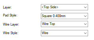
This tab allows you to set the default properties for a Bond Pad, used when added to your footprint.
This feature is available with the Chip On Board option.
Shortcuts
Default Keys: Shift+D
Default Menu: Setup
Command: Design Settings
Locating this option
Available from:
Setup menu > Design Settings option > Defaults > Bond Pad page
Setup menu > Technology option > Design Settings > Defaults > Bond Pad page
Using the Bond Pad Defaults Tab

When adding a Bond Pad to your footprint you will need an electrical Layer and Pad Style, but because the Bond Pad will also have an associated Die Pad with it, the default setting requires Wire Layer and Wire Style to also be defined.
Layer
The Layer that the Bond Pad resides on is selected from a drop down list defined in the Technology Layers dialog. This will be an electrical layer available from the Layers dialog.
Pad Style
Choose a suitable Pad Style for the Bond Pad from the drop down list defined in the Pad Style dialog.
Wire Layer
The Wire Layer is required because when adding Bond and Die pads, they are connected using a Wire, (Note, this is not the same as a Connection). Although the wire will not be plotted (generally), the wire must still live on a layer, hence a Wire Layer is defined. this would normally be a unique layer specific to Wires. It will also be defined as a Wire class when creating its Layer Class.
Wire Style
This will be style of the wire that connects the Bond Pad the its associated Die Pad. choose the Wire Style from the drop down list. As the Wire is generally not plotted, this style will be a suitable style (and hence thickness) that can be viewed in your design.
Related Topics
Technology Overview | Layers | Pad Style | Die Pad | Wire Layer | Wire Style | Insert Bond Pad | Insert Die Pad | Properties | Bond Pad Properties