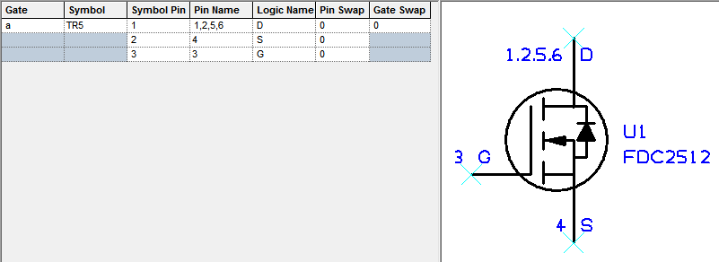
From the Gates page of the Parts Editor you can also map multiple PCB pins to the same Schematic pin. You might do this where one schematic pin represents multiple pins on a PCB Footprint, GND for example. This information will be available on each of the manufacturer datasheets, like for example, the Fairchild FDC2512 part.
Locating this option
Available from: Library Manager option > Edit button > Parts tab > Gates page
Mapping Multiple PCB Pads to same Schematic Pin
This allows you to model certain types of component that have ‘internal’ connections within them. It also allows those that have multiple internal pins that need to be assigned to the same net, for example, the ‘casing’ of some transistors. This is an alternative method to connecting pads together in the footprint by adding to the same net or using wires. The advantage of this method is that it means the footprint definition can remain neutral and generic, where the Part definition is made specific to a device.
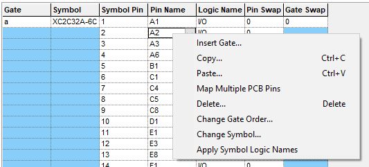
These mappings are made on the Gates page of the Part Editor. You will need to edit the Part that requires this mapping. On the Gates page, right click on the appropriate Pin Name cell and then select Map Multiple Pcb Pins from the context menu. Alternatively, with a Pin Name cell selected, the option is available from: Edit menu > Map Multiple Pcb Pins option.

This will turn the cell into an edit box instead of a drop down list to enable you to enter a list of PCB pin numbers. Type the Pin Numbers required into the list.

The list can be separated in two ways depending on how you want them to behave in the PCB:
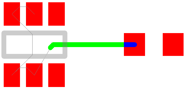
- The list can be separated with commas (,). This will assign all the PCB pads to the same net, with connections in the PCB that must to be routed until there are no net completion errors. For example, 1,2,5,6 When used in the PCB design, all the pads connected are displayed and can be routed to like the example below:

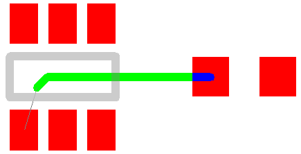
- Alternatively, you can use a plus sign (+) as the separator. This will assign the pins to the same net, by indicating that the pins are connected internally within the component and do not all need to be routed. For example, 1+2+5+6. However, when used in the PCB design, when routing close to an ‘associated’ pin, it will optimise to that net indicating a legal routing target as shown in the example below:

Note: If you wish to use alphanumeric names and map them to multiple pins, these names must first be added on the Pins page.
Related Topics
Parts Editor | Insert Gate | Change Gate Symbol | Automatic Gate and Pin Swap | Swap Gate | Swap Pins | Insert Part Representation