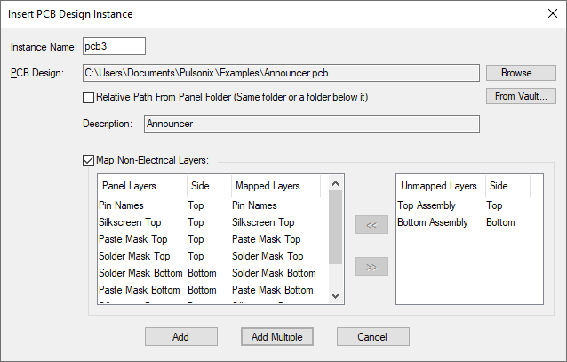
Use this to add an instance of a PCB design into a Panel design.
Shortcuts
Default Keys: None
Default Menu: Insert
Command: Insert PCB Design
How to Insert PCB Design Instances
First you will be presented with the Insert PCB Design Instance dialog to choose the required PCB design and map its non-electrical layers.

Each PCB instance added must have a unique name, enter the required name in the Instance Name box. These names are only used to uniquely identify each PCB instance in the panel.
Use the Browse button to choose the PCB design to place in the panel. Its file path and description will be placed in the dialog information boxes.
There are two ways of locating the PCB design file in the future when the panel design needs to access its data, for example when generating plots. The first way is to use its absolute file location. The second way is to access it in the same folder as the panel design, or in a folder below the panel design. Do this by checking the Relative Path From Panel Folder box. This is useful when saving the panel design with the PCB design, because if they are both then moved to a different folder the panel will still be able to find the design.
The number of physical layers in the PCB design, and the layer span structure must match the Panel Design. If they do not you will get an error message and not be able to add the PCB design. If the physical layers do match you will be given the choice of mapping the names of the non-electrical layers in the PCB design to the layer names in the panel technology data. If you do not map the names yourself, only the non-electrical layers with names that exactly match will be used when creating plots.
To map a layer name, select the PCB layer you want to map in the Unmapped Layers column, then select the panel layer you want to map to in the Panel Layers column and press the ”<<” button. If the sides are the same the layer name should move columns. To remove a layer name mapping select it in the Mapped Layers column and press the ”>>” button. It will move to the Unmapped Layers column. Any non-electrical layers left in the Unmapped Layers column will not be used for this PCB design when creating plots from the panel.
Press Add to add a single instance of the PCB design, or press Add Multiple to enter the Add Multiple Panel PCB Items dialog to add an array of PCB designs. You will now be able to position the PCB instance within the panel.
Right click to use the context menu to Rotate the PCB instance.
Left click to drop the PCB instance in the required position. Once the instance has been placed it can be repositioned by dragging the whole item.
Editing the PCB Instance
Once added to the panel design the individual PCB instances can be moved, rotated and aligned. By default, the origin of the PCB design is the bottom left corner of the board extents, but you can define a PCB Panel Origin in the PCB design using Place PCB Panel Origin from the context menu. The advantage of using a panel origin is when the PCB design is updated in the panel it will stay at the same place even if its board extents has changed.
Use Properties on selected PCB design instances to change the PCB Design file they refer to or to change the layer mapping.
Related Topics
Insert Panel Outline | Insert Panel Tab-Rout | Insert Panel V-Score | Panel Design | Add Multiple Panel PCB Items