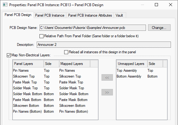
This dialog is displayed when the Properties option is chosen with a PCB instance selected in a panel design.
It shows and allows you to modify which PCB design is represented by the instance, and allows you to alter the non-electrical layer mapping for the PCB Design.
Shortcuts
Default Keys: I or Alt+Enter
Default Menu: Edit
Command: Properties
Locating this option
Available from: Edit menu > Properties option
Available from: Context menu > Properties option
Available from: Shortcut key > I
Using the Panel PCB Properties Dialog

PCB Design Name
This shows the name of the PCB design that this instance represents in the panel.
Change
Use the Change button to change this. Its file path and title will be placed in the dialog information boxes.
Locating the design
There are two ways of locating the PCB design file in the future when the panel design needs to access its data, for example when generating plots. The first way is to use its absolute file location.
The second way is to access it in the same folder as the panel design, or in a folder below the panel design. Do this by checking the Relative Path From Panel Folder box. This is useful when saving the panel design with the PCB design, because if they are both then moved to a different folder the panel will still be able to find the design.
The number of physical layers in the PCB design, and the layer span structure must match the Panel Design. If they do not you will get an error message and not be able to change the PCB design.
Description
Description is the description of the chosen PCB design.
Reload all instances of this design in the panel
By selecting this button, you can reload the selected design and all other instances of it into the panel.
Map Non-Electrical Layers
Use this section to set up the mapping of the names of the non-electrical layers in the PCB design to the layer names in the panel technology data. If you do not map the names yourself, only the non-electrical layers with names that exactly match will be used when creating plots.
To map a layer name, select the PCB layer you want to map in the Unmapped Layers column, then select the panel layer you want to map to in the Panel Layers column and press the ”<<” button. If the sides are the same the layer name should move columns. To remove a layer name mapping select it in the Mapped Layers column and press the ”>>” button. It will move to the Unmapped Layers column. Any non-electrical layers left in the Unmapped Layers column will not be used for this PCB design when creating plots from the panel.
Any changes to the mapping will be applied to all PCB instances that use the same PCB design.
Related Topics
Properties - Panel PCB Instance | Insert PCB Design Instance | Panel Design Overview