Pulsonix provides a powerful set of features to address advances in component and board technology. These features are available through additional licenses from your local sales office when you purchase the Advanced Technology cost option.
Flexi-Rigid Board Technology
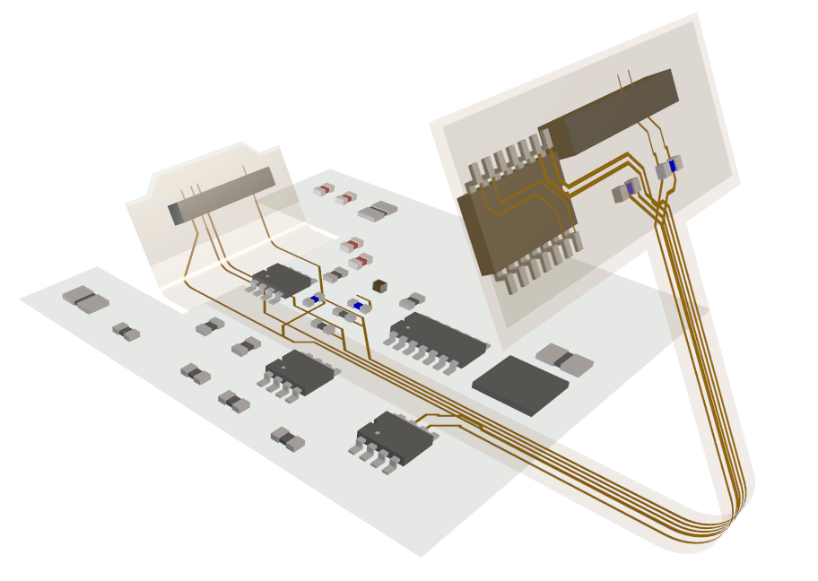
A Flexi-Rigid Board is generally a composite of rigid and flexi-board layers. Components can be attached to both the rigid and flexi portions of the design. More information about flexi-boards can be found on the Flexi Boards page.
This means the board outline is a different type on some layers, and also spans different layers. This can be achieved with the advanced technology feature by allowing a board to be on a layer span, and allowing Change Layer to place normal components onto the surface of the flexi-board.

Board Cavities
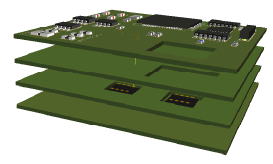
With this feature you can create Cavities (a cutout) in a board for a number of uses. For example, you may wish to use an Open cavity, one which exposes an inner layer to the surface. This may simply be a cavity for thermal properties or other uses. You may also drop a component into this cavity, a bare die which is connected to an outer layer using bond pads and wires, and then sealed using a bonding material. You may also use Internal cavities to create a cutout within two internal layers of the board. This may be used for inserting a thinned die or semiconductor into.

This is done by allowing a Board Cutout Area on a layer span. Components can then be placed within these cavities by using Change Layer.
Embedded Component Technology
This feature supports Embedded Component technology (ECT) such as printed and etched resistors, discrete embedded capacitors, buried capacitors, spiral inductors, RF components and embedded thinned die semiconductors.
Some specialist manufacturing processes allow you to place and embed components in the layer stack within the board. This technology allows much more efficient use of space, but requires additional features in the CAD system to enable this. Within the Advanced Technology option you have a set of features which enable the creation of special embedded component footprints and subsequent use of them within the internal layers of a PCB design.
For some embedded components, they may not have a body like conventional components, the functionality of the component is built into the board. Using copper shapes and perhaps resistive or capacitive materials inside the layers, these make up the component itself and are created during manufacture. There are many different types of embedded component, but they all have common requirements to enable them to be added to a design correctly.
With embedded components you can place pads and copper shapes on inner layers and create resist or coating shapes on layers which are embedded in the board stack. When you change the layer of such a component, you would want all the associated shapes to follow the pads. In a similar way to conventional technology, you can create additional non-electrical layers which are associated with an inner electrical layer. With this feature you can define an inner layer to be one on which embedded components are allowed to be placed. For embedded components to work correctly it is essential to define the design technology correctly before you begin to create the special footprints.
Chip-On-Board Feature
The Chip-On-Board functionality enables the support for single and multiple Chip-On-Board (COB) technology. Chip-On-Board is the use of a bare die directly onto the PCB substrate rather than using the traditional packaging of the device. Attaching a bare die directly to the board enables a large space saving; traditional packaging, even the very small ones still use significantly more space than this method.
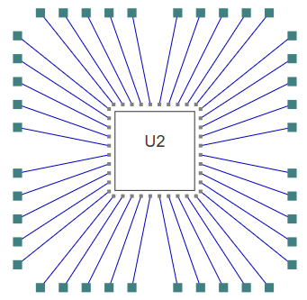
Within the Advanced Technology option you have a set of features which enable the creation of Chip-On-Board footprints and their subsequent use in a PCB design. Chip-On-Board technology in Pulsonix is made up of new design items, Bond Pads, Die Pads and Bond Wires. Bond pads are connected to Die pads using a bond wire and they will share the same pad number. Unlike normal component pads, bond pads can be moved independently of other pads in the same component in the PCB design.

Die pads differ from normal component pads by being placed on a Wire layer, a “pseudo” electrical layer that is used to hold items that are outside of the surface of the board. You can connect to die pads, but they are not plotted with the other electrical items. Bond Wires are also not normally plotted but you can extract a report of the wire start and end positions for use with automatic wire machines.
Chip-On-Board Feature Detail:
-
Within footprints, add bond pads using Insert Bond Pad and add die pads using Insert Die Pad.
-
For the Die and Bond pads to be connected together use a Wire so that they have the same net name. During Insert Die Pad, a bond pad is automatically added with a connecting wire.
-
Automatic rotation of the bond pads is possible during positioning around the shape or during interactive moving of the bond pads.
-
Use the Properties dialog to convert from a normal pad to a Die Pad by changing its layer to a wire layer.
-
Use Place Bond Pads to place bond pads around a user defined shape for specific positioning.

-
In the PCB design editor, you can move bond pads on components independently of the die component body (normal pads are in fixed positions).
-
Four options are available from the shortcut menu when selecting a component with die and bond pads in a PCB design. Select All Bond Pads will change the selection to just all the bond pads, use Reset Bond Pads to reset all of the bond pads to their original position, Move Chip Body will allow you to position the component without changing the positions of any of the bond pads. You may do this following accurate positioning of the bond pads, and use Change Chip Body Layer, if available, to move the chip body onto another layer. For example to move the body into a cavity and leave all of the bond pads on the top side. This is only available if the board has a suitable layer to move it to that allows normal components on it.
-
Specific rules exist for use with the Chip-On-Board feature and are used during Online DRC or batch Design Rule Check. You can define the Minimum and Maximum Bond Wire Length and the Minimum Die Pad Space.
-
Use the Library Generator toolkit to write an import file for importing components containing Bond pads, Die pads and connecting Wires.
Where no license is available for this option but the design has used specific Chip-On-Board design items they can be viewed but not manipulated. Parts created which use PCB Footprints specific to Chip-On-Board technology do not affect the Schematic design editor, they will use normal Schematic Symbols but the translation of the design to the PCB design editor will need the Chip-On-Board feature.
Related Topics
Bond Pads | Embedded Components | Technology - Spacing Rules | Die Pads | Flexi-Rigid Board | High Speed Cost Option | Micro-vias | Place Bond Pads