Use this tool to create a new Schematic from a PCB design. This process is useful if you want to document a PCB design with no schematic, for example a prototype board.
Shortcuts
Default Keys: None
Default Menu: Tools
Command: Reverse Engineer
Locating this option
Available from: Tools menu > Reverse Engineer option
How To Use Reverse Engineer
You should ensure that your library contains all the appropriate gate symbols and that they are referenced by the parts used in the PCB. Otherwise, the gates for some parts will be assigned generated symbols. Parts with no gates defined are assumed to be PCB only and will not be translated at all.

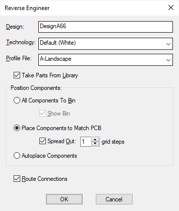
Design
The name of the Schematic design, which would normally be the same as for the PCB.
Technology
Choose a Schematic Technology to use. The technology defines the styles, etc to be used.
Profile file
Choose a Schematic Profile to use. This will give you a jump-start, because you can have your sheet outline and other general annotation predefined.
Take Parts From Library
Check this to ensure the schematic will use the latest parts from the Pulsonix set of part libraries. Leave it unchecked to use the parts from the PCB design, for example if the appropriate part libraries are not available.
Position Components
Choose from the following three methods of positioning the components in the schematic design:
-
All Components to Bin
Check this option if you want to use the Component Bin. Otherwise connected components are placed in the design area.
Note that connected components are put into a special Used section of the bin containing connected items. Once these components are removed from the bin that cannot be put back in, unless they are disconnected.
Show bin
Show the Component Bin. Use this if you are putting the components into the bin to make sure it is displayed and ready for use when you edit the generated schematic design.
-
Place Components to Match PCB
Check this option if you want the components to be, as closely as possible, in the same place as in the PCB design. This is a good starting point for easily finding components as you know the PCB design and then placing groups of related items onto new pages. It will place the centre of each schematic gate in the exact same position as the centre of the corresponding component in the PCB design. If a schematic component has multiple gates, they will be placed side by side, centred at that position. Two pin components will be automatically mirrored and/or rotated to have the same orientation as the PCB component. After placement the components will be moved to the centre of the working area, any components still off the working area after that will be placed in the bin.
Spread Out
Check this box to move the schematic gates on to the Component Grid and spread them out so that they do not touch. Type the number of grid steps required between items to ensure they are spread out and have space around them. This will make it easier to route the connection paths.

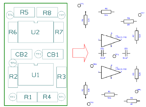
The above illustration shows a small sample PCB before, and the Schematic design after the use of Reverse Engineer and Place Components To Match PCB with the Spread Out option selected.
Leave unchecked to centre the components exactly where the PCB components are, possibly on top of each other as the gates may be bigger than the PCB footprints. You can always create space later using the interactive Spread Out function.
-
Autoplace Components
Check this option if you want the connected components automatically placed in the design area, minimising the straight line connection lengths between them.
Route Connections
The program will attempt to route the connections. Any which could not be completed will be draw as straight point to point connections and drawn in the unfinished colour. For power nets, the net name will be displayed next to each pin. The router will give you a head start, but you will probably want to tidy the design by hand. Obviously, this option has no effect if the components are placed in the bin, and will have limited success if the components are placed to match the PCB without spreading them out.
Placing Symbols
When manually moving symbols after reverse engineer there is a useful switch in the Options - Edit Connection dialog called Show Connection To Nearest Node. Use this to show a temporary line from any moving pin that is on a net but does not have a connection attached to it. The temporary line will end on the nearest static item that is on the same net. This is to indicate where the symbol is best placed to be close to other items on the same net.
Related Topics
Design Settings - Synchronisation | Parts Editor | Parts Editor - Gates Page | Component Bin | Show Connection To Nearest Node | Spread Out | Translate to PCB