ODB++ is a CAD/CAM data exchange format which can be used as an alternative to Gerber and Excellon.
Shortcuts
Default Keys: None
Default Menu: Output
Command: ODB++
Locating this option
Available from: Output menu > ODB++ option
Description
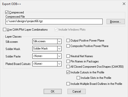
This option is driven from a single dialog, accessed by selecting the ODB++ option from the Output menu.

ODB++ can be output in two forms
- Folder Structure All the individual files are held in a structured folder format.
- Compressed All the data is compressed into a Tar format file with the file extension .tgz.
Checking the Compressed check box indicates that the data will be output in tar format.
Use Browse to change the destination of the compressed file or where the folder structure is to be located.
Checking the Use CAM/Plot Layer Combinations check box means that instead of outputting data for every layer in the design, it will output data for each Gerber and Excellon type plot defined in the CAM Plots page of the Technology dialog. Windows plots will be included if Include Windows Plots is checked. If you have variants defined for you CAM Plots, the contents of the ODB++ file will use the layer and the Variant defined for it.
Within the ODB++ file exported, the special Component Top and Bottom layers use the current variant in the design.
Layer Classes
In the ODB++ format the Silkscreen,Solder Mask and Solder Paste layers need to be identified. Use the appropriate drop down list to select the layer class which will identify these layers. You can select (None) if you are not interested in the layer type.
Power Planes
Power Planes are always output in the negative format. If your manufacturer requires a positive version of the layer as well select Output Positive Power Plane. This will not appear if you are using CAM/Plot Layer Combinations.
If you have tracks buried in your Power Plane layers, selecting Composite Positive Power Plane will replace the negative version of the plane with a composite of the positive and negative plots.
If there are no power planes in the design these options are not displayed.
Neutral Net Names
If this is checked then all user defined net names will output as numerical net names. This can be used to hide company specific net names.
Pin Names in Packages
Checking this means that pin names rather than pad numbers are output in the package data in the EDA file. This is required by certain applications.
All Closed Component Doc Shapes (CAM350)
In general, only one closed documentation shape is output to the comp_+_top and comp_+_bot plots. CAM350 allows more than one shape for the component shape and some of its processes require this. Check this option if you require this.
It should be noted that more than one viewer will reject the ODB++ design if there are more than one shape specified for each footprint definition. This should ONLY be checked if you are sure that your process can handle this.
Include Cutouts in the Profile
In the ODB++ format, the board outline is defined and drawn as a ‘Profile’. This switch will enable the output to also apply Cutouts to the board (Profile). Some of the later versions of the ODB++ viewers have the ability to read cutouts in Profiles.
Include Slots in the Profile
This switch is only available if Include Cutouts in the Profile is checked. It will enable the output to apply through-hole slots as cutouts to the board (Profile) instead of adding them to the drill layer. Some ODB++ tools prefer to read slots in Profiles rather than as oval features on a drill layer.
Include Multiple Board Outlines in the Profile
In the ODB++ format, the board outline is defined and drawn as a ‘Profile’. Most ODB++ viewers require the profile to be a single shape, but some ODB++ viewers have the ability to read multiple boards outlines in Profiles. Check this switch to enable the output of all board outlines in a PCB design to the Profile, if unchecked only one of the board outlines will be included.
Drill Types in the ODB++ Export
If you have defined a Drill Type in your Pad Styles, then the formatting of the Type name must follow the ODB++ naming convention. See the Pad Styles page for more information.
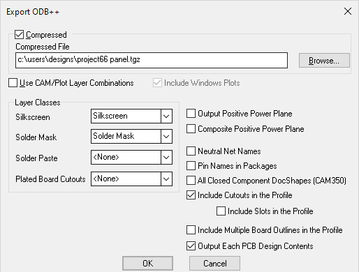
For Panel Designs
Output Each PCB Design Contents
This check box is only shown if you are producing output for a Panel Design. Use Output Each PCB Design Contents to specify that each PCB item in the panel will be replaced by the full contents of its PCB design file. Leave it unchecked if you are just producing a quick check panel output and only want to output the items you see in the PCB instances in the panel design.

ODB++ Viewers
There are ODB++ viewers available so that you can check the output. Depending on the viewer you may have to change from the compressed to the non compressed form. You may also have to uncheck the switch Include Cutouts in the Profile if your viewer is an older one, see above.