The Technology files hold all the essential parameters that go to make-up a design. For example, in Schematics this would be the line widths, junction point styles, text styles, attribute names, etc. In PCB these would be track widths, pad styles and sizes, spacing rules, net names and classes, number of electrical layers, documentation layers, power planes, etc. You can also define design rules. Some rules can be passed from the Schematic to the PCB. By using standardised naming conventions it is possible to define generic rules in your Schematic technology which will ultimately drive the PCB design process.
In Pulsonix these are all held together under a specific Technology file name. You may produce as many different Technology files as you wish using your own naming conventions. This then becomes a powerful concept. Each time you open-up a new design you firstly select the appropriate Technology from the files of different Technologies prepared as you build up experience with Pulsonix. Straight away you are on the fast track as your new design project is fully setup ready to start designing with all the correct parameters.
Using the same Technology contents, especially Layer setup, for creating both library items and designs, will allow for consistency and standardisation.
Some Basic Technology Files Example
Example 1
Typically, this example provides reasonably thick tracks and spacings for through hole technology. The values below are shown in Imperial (thou) units:
| Track width | Track clearance | Pad width | Pad clearance | Via width | Hole size | Layers |
| 12 | 12 | 55 | 12 | 45 | 28 | 2 |
Example 2
This example would provide you with a through hole technology and two tracks between pads.
| Track width | Track clearance | Pad width | Pad clearance | Via width | Hole size | Layers |
| 10 | 10 | 50 | 10 | 40 | 24 | 2 |
Example 3
With this technology example, 3 tracks between pads is possible using a off-grid track grid or thicker tracks on less dense SMD designs.
| Track width | Track clearance | Pad width | Pad clearance | Via width | Hole size | Layers |
| 8 | 8 | 50 | 8 | 40 | 24 | 4 |
Example 4
An example technology for fine line designs, suitable for SMD work.
| Track width | Track clearance | Pad width | Pad clearance | Via width | Hole size | Layers |
| 6 | 6 | 40 | 6 | 35 | 18 | 6 |
These simple examples are very limited and basic, giving only one parameter for each design element. In reality the design may have several different track widths and perhaps 20 different pad styles to choose from. The important thing is to understand the concept. Let us look at a real Technology file:
How to open the Technology file
From within a Schematic or PCB design, from the Setup. menu, select the Technology option.
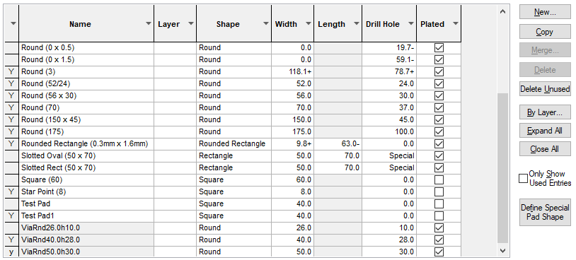
The tabs on the right side of the Technology dialog separate all the individual aspects of the design technology, for example, Pad Styles. Here are all the Pad styles available in this particular Technology. The file may be easily amended, adding, deleting, or modifying the Pads within a Technology, or in order to create a completely new Technology file.

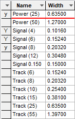
This example below, shows various Track Style widths allowed for this particular Technology file.

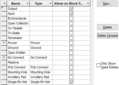
An example of a Schematic Technology file is shown below, this displays the Pin Type Rules page:
