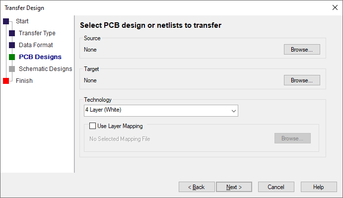
This enables you to select one or more PCB designs or PCB netlists that you want to translate into the Pulsonix PCB format, and also which file or folder that you want to store the translated designs.

Source
This specifies the source PCB designs that you want to transfer. Use Browse to select the designs. You can select more than one design to transfer but they must all be in the same folder.
Once you have selected one or more design, the target design names will default to the selected names with specified Pulsonix PCB design extension.
Target
This specifies what the transferred designs will be. If you have selected just one file to transfer, you can use Browse to change the name and or the folder of the target filename. If you have selected multiple designs, Browse can be used to change the folder that the transferred files go into. You cannot change the name of the transferred designs if you have chosen multiple designs.
Technology
You can specify a PCB technology file to use for the transfer. If you specify a technology file to use, then the transfer will use appropriate styles and rules from the technology file.
For some vendors it is more appropriate to use no technology file as the styles and rules are defined within the design.
If you have selected a technology you can use check Use Layer Mapping which will allow you to map the other EDA systems layers to the Pulsonix layers specified in the technology files. Use Browse to select the mapping file that you want to use. The mapping file needs to have been created from importing a file from the EDA system and checking Use Layer Mapping.Then Layer Mapping will be activated before the import starts, and you can set up the mapping file.