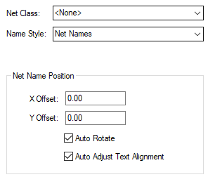
This tab allows you to set the defaults for a net. In particular, how net names will be displayed on the net.
Shortcuts
Default Keys: Shift+D
Default Menu: Setup
Command: Design Settings
Locating this option
Available from:
Setup menu > Design Settings option > Defaults > Net page
Setup menu > Technology option > Design Settings > Defaults > Net page
Using the Net Defaults Tab

Net Class
This enables you to select a default
Technology Net Class from the drop down
list available. this is used when adding a new
Connection or
Track to the design. If you do not wish to use a
Net Class, select
Name Style
This will be the Text style of the Net Name when displayed in the design. Select the style using the drop down list of text styles defined in the Technology Text Styles dialog.
Net Name Position (SCM only)
The Net Name Position box allows you to set up the offset to be applied when calculating the position for new net names to be displayed on pins, junctions and bus terminals.
The Offset is applied to the centre of the pin, or the connection end of the bus terminal. The direction to apply the default offset will be calculated to run along any attached connection. If there are no attached connections and the node is a pin, it will work out the direction from analysing the symbol to see which side the pin is on. The new net name will have its offset extended if it needs to avoid the pins already displayed pin name or logic name.
Check the Auto Rotate box if you want the net name to have its rotation changed to 90 degrees to lie along a vertical connection attached to the node, or if the node has no connections and lies at the top or bottom edge of a symbol.
Use Auto Adjust Text Alignment to specify if the net name can have its Text Alignment altered to be at the corner of the name box that is closest to the pin or bus terminal. This has the advantage that if the net name is changed or its style is changed, its offset to the parent node is always kept the same.
Name Layer (PCB only)

In addition to the controls above, in a PCB design, you can also specify the Name Layer. This is selected from a drop down list defined in the Technology Layers dialog and can be any layer in the design. This Layer will be used when be used when the Show Net Name option is selected from the context menu for a selected Net or Track.
Related Topics
Technology Net Class | Technology Layers | Technology Text Styles | Net styles Defaults | Insert Connection | Insert Track