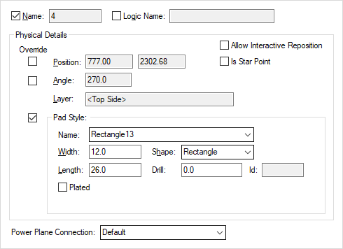
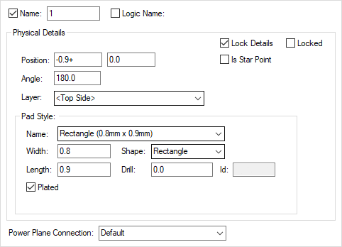
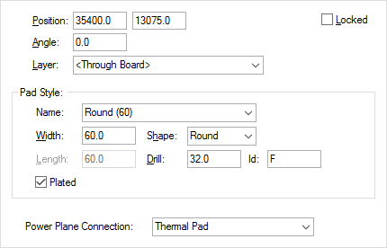
This dialog is displayed when the Properties option is chosen with a Pad selected. Pads may be pads on PCB footprints or Free Pads.
It shows and allows you to modify properties for the selected Pad.
Shortcuts
Default Keys: I or Alt+Enter
Default Menu: Edit
Command: Properties
Locating this option
Available from: Edit menu > Properties option
Available from: Context menu > Properties option
Available from: Shortcut key > I
Using the PCB Pad Properties Dialog

Physical Details
Name is the pin number of the selected Pad. Check the control on the left to display the pin name.
If editing a component pad the Override and Allow Interactive Reposition check boxes will be available. Normally component pads in a design would not have their position, layer and style changed from those defined in the footprint, but occasionally this might be required. Check the appropriate Override boxes to allow changes to the property to their right. Uncheck the Override boxes to return the values to those defined in the footprint.
Selecting the Allow Interactive Reposition check box to will allow repositioning of component pads during interactive operations such as move and align. With this unchecked, the pad will be locked against interactive repositioning. When a component with pads is added to the design, all pads will initially have Allow Interactive Reposition switched off, and so they cannot be accidentally moved in the design.
Position and Angle display positional information about the Pad in the current design units.
Layer displays the Layer used by the pad.
The Pad Style controls display information about the pad style used by the selected pads. If editing a component pad these controls can not be changed unless the Override box is checked. Once enabled, the Name: can be selected from the drop down list box or by interactively typing the Width, selecting a Shape from the drop down list, or by typing the Length, or the Drill size. The Plating Status: check box will be available if the Pad Style check box has been selected. If there is no Pad Style to match these parameters then a new Pad Style will be added with the name that you want to call it. For a component pad, uncheck the Override box to return the values to those defined in the footprint.
Power Plane Connection
Power Plane Connection allows you to specify how the pad would connect to a power plane or poured copper. The default is to create a Thermal Pad as specified in the Thermal Rules. Alternatively, you can specify that the pad is fully connected or completely isolated from the plane. If it is completely isolated, the gap is determined by the Pad to Copper spacing rules.
If the Pad Style has a Spacing Shape defined for the current layer, then this will be used to determine the shape around the pad, instead of the actual pad land shape. This can be disabled by selecting the connection type Thermal Pad (ignoring Spacing Shape), this does not disable the Spacing Shape for any other spacing or rule checking process.
Allow Suppress Lands
When enabled will allow a land to be suppressed when appropriate (i.e. the layer has Suppress Unconnected Lands enabled and this pad is not connected on that layer). Uncheck this option to not allow any land suppression on this pad.
Pin Network

If Pin Networks are defined in your technology, then you will be able to add a pin network to the selected component pad by selecting it from the Pin Network control.

If the selected component pad is part of a pin network, then the properties page will show the name of the network, the name of the Master component pad, and any length restriction which may apply. Only the length restriction can be changed through the properties page. The length restriction shown in this dialog is what will be used during checking. Changing the value in the Pin Network definition in the technology does not change the value here.
The Reset to Default button will attempt to reset the length restriction value to that defined on the Pin Network in the Technology.
Using the PCB Footprint Pad Properties Dialog

If you want to lock the physical details of the footprint so they cannot be overridden using the PCB Pad Properties dialog, then check the Lock Details box.
Using the PCB Free Pad Properties Dialog

If want to change the pad style of the Free Pad then you can change it to a another predefined Pad Style by selecting one from the Name drop down list.
You can alternatively change it to a new Pad Style by defining alternative parameters. This can be done by changing the Width and or Length, or the Drill size, or by changing the Shape drop down list. If there is no Pad Style to match these parameters then a new Pad Style will be added with the name that you want to call it.
If appropriate, the drill identifier assigned to the current drill size is shown next to the drill diameter.
The position of Free Pads can be change by typing different coordinates into the Position edit controls.
The Layer of the pad changed by selecting another layer name from the drop down list.
Free Pads can be locked or unlocked against repositioning by checking or unchecking Locked .
Related Topics
Pad Styles | Thermal Rules | Pour Copper | Pin Networks | Drill Size Table