Pulsonix supports Embedded Component Technology (ECT) such as printed and etched resistors, discrete embedded capacitors, buried capacitors, spiral inductors, RF components and embedded thinned die semiconductors.
Some manufacturing technologies allow you to embed components in the layer stack. This allows much more efficient use of space, but requires additional features in the CAD system to allow components to be placed within the board.
In a conventional PCB design, components can only be added to the Top or Bottom sides of the board. A conventional footprint will have a body which is placed above the surface of the board and pads which fit onto or through the board. You would normally have the following items in a footprint: a silkscreen outline which is associated with the top side (flipped to the bottom when component is placed on the bottom); a placement area which represents the space needed to accommodate the body of the component and is either through the board, or just on the top (and flipped when on the bottom); pads (though hole or surface mount); resist shapes, which are often generated from the oversized pad shapes.
In a conventional technology, you would define Silkscreen, Resist and Placement non-electrical layers which are associated with the Top and Bottom electrical layers.
Embedded components, may not have a body like conventional components, the functionality of the component is built into the board, using copper shapes and perhaps resistive or capacitive materials which are applied to the board during manufacture. There are many different types of embedded component, but they have requirements in common to enable them to be added to a design.
With embedded components you may want to place pads and copper shapes on inner layers and create resist or coating shapes on layers which are embedded in the board stack. When you change the layer of such a component, you would want all the associated shapes to follow the pads.
In a similar way to the conventional technology, you can create additional non-electrical layers which are associated with an inner electrical layer. You can also define an inner layer to be one which embedded components are allowed to be placed on. For embedded component to work correctly, it is essential to define the design technology correctly before you begin to define the footprints.
If you are using embedded components, it is likely that you may also want to use blind or buried vias which are only partly drilled through the board. You can do this by defining layers spans which define the spans which can be drilled. You may also want to consider Micro-vias.

Overview of the ECT Process
To use embedded components you must first create the technology to support this feature before creating the embedded component footprints.
- Edit or create the Technology File that you wish to use. This will be used for the design and to create the footprint. It should contain suitable Layer Classes, Layers, Materials, Layer Spans, Pad Styles (vias) and Net Styles.
- Add Layer Classes to support embedded component technology. For layers that are critical to the final manufacturing process, select the Essential For Manufacturing check box in Layers Classes dialog.
- Add Inner Electrical layers and allow Associated Layers. Also enable Allow Buried Components for the electrical layer containing the embedded component.
- Add non-electrical inner layers to support embedded component manufacturing and documentation processes.
- If your embedded component is to be placed into an internal cavity, create a Layer Span to define the depth of the cavity.
- Create your footprint and save it using the Embedded Component check box on the Save to Library dialog. Make sure you create an Area defining the Component Body on the layer you want to place the component on, and add a board cutout area if the component is to live in an internal cavity.
- Create your design using the same technology file as used for creating the footprints. Add the embedded components. If there are more than one internal layer suitable for the components use Change Layer to place the components on the correct layer.
Examples
Embedded Resistors

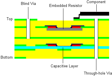
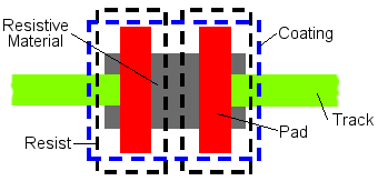
A printed resistor consists of two pads, connected by some resistive material. Depending on the manufacturing method, a resist mask or encapsulating coating may also be required. The technology would therefore require an electrical layer with associated non-electrical layers for the resistive material, resist and coating shapes.
If we wanted to place these embedded resistors on electrical inner layer 1 we would first define this layer as one which Can Have Associated Layers and as one which can Allow Buried Components. Then create the appropriate non-electrical layers, and Associate them with the inner layer. It would be appropriate to define the layer class for these non-electrical layers as Essential For Manufacture, this would prevent the component from being added to electrical layers which do not have these associated layers present. Using this technology, a footprint can be created with the appropriate shapes. This footprint should be marked as for an Embedded Component, this tells the system that it is a footprint which can be placed on inner layers. If more than one set of appropriately defined layers exist, change layer can be used to move the footprint through the layer stack.
Embedded Capacitors

This embedded capacitor consists of two pads on two individual layers, separated using dielectric material. One of the layers (marked as Capacitor in our example) would be specifically used for landing pads to one side of the capacitor. This would be isolated from the other capacitor pad with a thin dielectric construction layer. The Capacitor and Dielectric layers would be constructed during manufacturing using a build up technique which would add no significant thickness to the Electrical layer Inner 2. The Capacitor would be a thin copper foil applied to the pad areas where the capacitor is defined.
Create layer Inner 2 as an internal electrical layer that Can Have Associated Layers, is Top Facing and can Allow Buried Components. The Capacitor layer has a number of important elements to make it function correctly; it should use an electrical Layer Class that has Physical Copper Layer unchecked (not selected). This layer will not be plotted and will not allow tracks. Only the Micro-via layer span (shown in the diagram) will connect to it. Within the Layer itself, Can Have Associated Layers is selected to make the layer Top Facing.
Planar Converter (Planar Transformer)

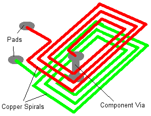
A third example of an embedded component shows a planar converter. This component spans any number of layers in the design and may have physical body applied to the outer layers. However, part of the footprint consists of copper spirals which are connected by a Component Via, effectively joining the two footprint pads. Although the pads are joined we would want to connect them to different nets. We can do this because it is possible to mark the copper spirals and component via as not checked. A Component Via is a fixed part of a footprint, but unlike a pad or mounting hole, it does not have a pin number and it exists on a layer span, like a normal routing via. If we defined this footprint but did not mark it as embedded, mirroring the component would not swap the inner electrical layers. By defining the footprint as embedded, you can mirror the component and all the inner layers will swap as expected.
Embedded Semiconductors and Thinned Dies
The last example of an embedded component shows embedding a Thinned Die into a cavity in the core. To do this you have to create two pseudo electrical layers for the top and bottom of the Core containing the cavities. These layers are not marked as Physical Copper Layers and are not usually plotted. They are used in the footprint for drawing the component pads on and in the PCB design for defining the stop pad side of a micro-via span. The layers can also be used to create a layer span to be used for board cutout areas within the footprint.
Create a Component Body area in the footprint on the lower of the pseudo electrical layers, give it a height and do not forget to mark the footprint as an Embedded Component. When added to the PCB design using the same technology, the component will be placed on the same lower core layer its body was defined on, which is bottom facing, but the component will be marked as not mirrored as it sits in the cavity in the core.
Related Topics
Technology - Layers | Technology - Layer Class | Technology - Layer Spans | Board Cavities | Micro-vias | Change Layer
Footprint Editor - Symbol Properties | Properties - Shape | Properties - Component Via | Insert Pad | Insert Mounting Hole | Insert Via | Insert Spiral