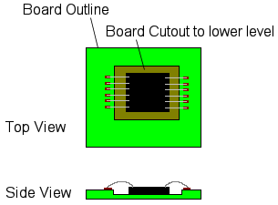
Cavities are cutouts in the board outlines that only exist on some of the layers. You can create cavities in a board for a number of uses. For example, you may wish to create an Open Cavity, one which exposes an inner layer to the surface. This may simply be a cavity for thermal properties, or you may want to drop a component into it, maybe a bare die which is connected to an outer layer using bond pads and wires and then sealed using a bonding material.
You may also wish to use an Internal Cavity to create an embedded hole between two internal layers of the board. This may be used for inserting a thinned die or semiconductor into. Generally, the internal cutout would not be left void without anything actually filling it.

The first stage in defining a board cutout as a cavity is to define a layer span for the cut away layers. Next add a Board Cutout Area on this layer span to produce a cavity.
For an Open Cavity you can define the exposed layer as one allowing Normal Components. It would then be legal to place a surface mounted component on that layer within the cutout area. This is done by using Change Layer on the component.
To place through-hole components into an Open Cavity, a layer span will have to be created from the exposed layer through to the other side of the board. The component should then be placed onto that layer span. Each of the through-hole pads will be automatically changed to be on the new span.
Any component still on the Top or Bottom layer of the board, but inside a cavity will be marked in error by the Component Spacing Design Rule Check. Similarly, components that have been changed to the cavity layer, but have not been moved into the cavity area will also be checked.
For an Internal Cavity you can define the lower layer of the cavity layer span as one allowing Buried Components and you can create a specialised embedded component to be placed into the gap. See the section on Embedded Components for more details.
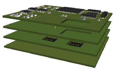
The picture below shows two components within internal cavities within the board structure. Additional cutouts above the right hand component illustrate a component exposed to the surface through the use of multiple board area cutouts on spans.

Related Topics
Embedded Components | Flexi-Rigid Boards | Change Layer | Insert Area | Insert Board | Technology - Layers | Technology - Layer Spans