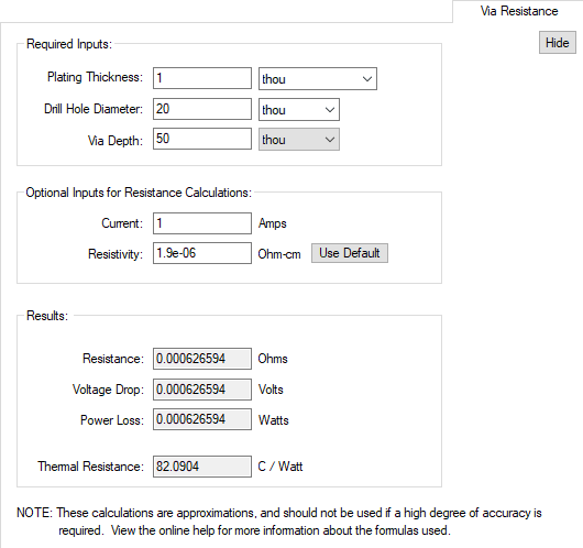
This is a calculator to calculate the resistance, voltage drop, power loss and thermal resistance of vias in a PCB design. It has the ability to take the hole diameter and other parameters from a via selected in the design.
Shortcuts
Default Keys: None
Default Menu: Utilities
Command: Design Calculators
Locating this option
Available from: Utilities menu > Design Calculators option
Using this option
This calculator is on a tab on the Design Calculators dialog, available from the Utilities menu. The following dialog appears when the Via Resistance tab is selected.

Required Inputs
The values in this section are required to calculate the thermal resistance and the resistance for the via.
You can automatically enter some values in the dialog by picking on a via in the PCB design. To do this, move the cursor out of the dialog and you will be presented with a calculator cursor. Use this to pick on the via in the design and any information that can be extracted from it will be automatically entered into the dialog. Extracted values will be presented in bold text in the dialog.
If you can not see enough of the design, use the Hide button at the top right of the dialog to hide the dialog until the mouse key is clicked. In the hidden mode the calculator will work “On-The-Fly” and will present the results from the via the cursor is hovering over in a tooltip window. Click on a via, or use the “On-The-Fly” command from the context menu, to see the full dialog again.
Plating Thickness
Enter the thickness of the copper the via is plated with, and select the units the value being entered is using. You can choose to define the thickness using ounces per square foot, which we equate to thickness using 1.378 thou per oz.
This value will be automatically taken from the thickness of the Material that has special use Hole Plating or Micro-Via Hole Plating, dependent on the type of via selected.
Hole Diameter
This is the drill diameter before plating is applied. You can also enter this value by picking on a via in the PCB design and its drill size will be automatically entered into the dialog.
Via Depth
Enter the length of the via through the board. If you have a complete layer stack defined with thicknesses the via depth will be calculated from the span of the picked via.
Optional Inputs
The Resistivity in this section is required for calculate the via Resistance, and the applied Current is required to calculate the expected Voltage Drop and resultant Power Loss.
The Resistivity value will be automatically calculated from the Electrical Conductivity of the Material that has special use Hole Plating or Micro-Via Hole Plating, dependent on the type of via selected.
If this is not set up and you do not know the plated copper Resistivity, it can be set to the default value of 1.9e-006 by pressing the Use Default button.
Results
Once legal values have been entered for all input sections the results will be automatically calculated. The fields will be left blank if not enough information has been entered. The formulas used to generate these results are detailed below.
Formulas
The formula for thermal resistance used in this calculator is:
Thermal Resistance = (Thermal Resistivity * Via Depth) / Via Area
where:
Thermal Resistivity for plated copper is assumed to be 0.249 cm-K/W (at a temperature of 300K)
Via Depth is the length of the via through the board, entered directly in the dialog.
Via Area is the cross section of the plating, defined by (PI * (Drill Diameter - Plating Thickness) * Plating Thickness)
The formula for via resistance used in this calculator is:
Resistance = (Resistivity * Via Depth) / Via Area
Voltage Drop = Current * Resistance
Power Loss = Voltage Drop * Current
where:
Resistivity is the plated copper resistivity entered in the dialog, and defaults to 1.9e-006.
Via Depth and Via Area are as mentioned above.
Current is the current applied to the via in amps, entered directly in the dialog.
NOTE: These calculations are approximations, and should not be used if a high degree of accuracy is required.
References
“Constructing Your Power Supply - Layout Considerations”, by Robert Kollman
“Current Carrying Capacity of Vias”, by Doug Brooks and Dave Graves
“Appendix B”, Materials Science and Engineering - An Introduction, by William Callister
Related Topics
Conversion Calculator | Heat Sink Calculator | RLCF Calculator | Scientific Calculator | Track Impedance Calculator | Track Width Calculator