The Design Level Spacing Rules dialog is used to define the default minimum distance between items for a design.
A detailed description of how spacings are determined is given here.
Shortcuts
Menu: Setup
Default Keys: T
Command: Technology
Locating this option
Available from: Setup menu > Technology > Spacing Rules - Design Level page
Using the dialog
To display this dialog, select Technology from the Setup menu, (or use the shortcut key or toolbar icon), then select the Design Level tab in the Spacing Rules section.
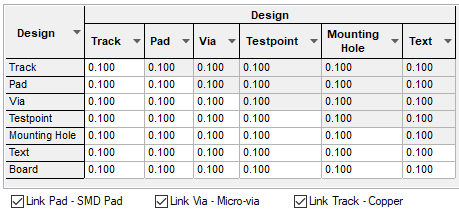
The top right section of the grid is greyed out because spacings between types of items are reversible.
The design level spacing values are presented in a grid, allowing you to easily change the values directly. Click on the text of the value you wish to change, and edit the text to show the required value. You can also take the value from one cell and apply it across the whole row, down the whole column, or to all the cells of the whole grid, by pressing the right-hand mouse button and selecting the required option from the context-sensitive menu. Greyed out cells cannot be changed because the reverse spacing is equivalent (i.e. Track to Pad is the same as Pad to Track).
The Spacing Rules page for a PCB design is shown below. The page for a Footprint is similar, but only contains the items relevant to a Footprint design.

The above page represents Design Level spacing rules. If you wish to create more refined rules, the Net Class Level or Match Pair Level rules dialogs can be used.
The Check Spacing Values dialog is used to show you the actual spacing used between items on two specified Net Classes.
Linked Types
These are enabled using Design Settings - General - Spacing Rules - Enable linking of types. When this is done, some rows and columns on the spacing grid will disappear (provided the spacings are the same), and the values are linked together. You can show the hidden values by unchecking the appropriate options which appear under the spacing grid. You can link Pad - SMD Pad, Via - Micro-via, Track - Copper.
Additional Design Level Spacings and Rules
There are a number of item specific spacing rules, outlined below.
Board
Use Board Centreline - Check this box to ignore the width of all board outline shapes. Checking would then be done upto the centreline of the shape.
The Min Board To Board spacing would normally be set to zero if using V-Scoring or the Tab-Rout line width (i.e drill size used to mill it) if using Tab-Routs.

Bond and Die Pad
Bond Wire Length
This is the Minimum & Maximum length of bond wires. A value of 0 means unrestricted.
Die Pad Space
This is only available in the PCB and footprint editors, and defines the Minimum distance between die pads.

Component
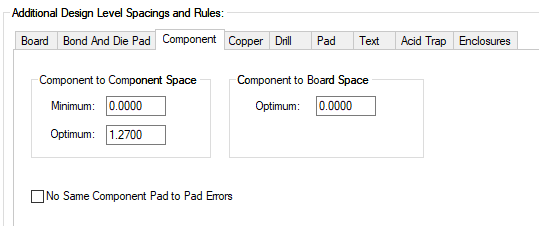
You can specify rules relating to the spacing of components. The area occupied by a component is determined by the component body areas defined in the footprint. If the component does not have any body or clearance areas, the bounding box of any documentation (e.g. silkscreen) shapes is used.
Component to Component Space
The Minimum space is used by Design Rule Check to look for overlapping components. The Optimum space is used when using Push Aside whilst manually moving components, and by Auto Place, in order to space the components out a little.
Component to Board Space
The Optimum space is used when using Push Aside whilst manually moving components, and by Auto Place, in order to keep the components away from the edge of the board.
No Same Component Pad to Pad Errors - Check this box to ignore pad to pad errors within the same component footprint (or documentation symbol), this also includes mounting holes.
Copper
If the Check between hatch lines option is checked, the Net Connectivity Checks and Optimise Nets functions will check that there is no break in connectivity as a result of items falling between hatch lines. Spacing checks will consider the gaps between hatch lines, so items placed between them will not result in a spacing error. Pour Copper will not place an isolating cutout around an item, unless that isolating shape connects to the hatch lines.
This additional checking has a performance penalty, but should be used if you are using hatched copper with a large separation between lines. When this option is not checked, hatched copper is considered to be a solid shape and any item within its perimeter is connected.

Drill
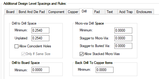
Drill to Drill Space
The minimum distance between the outer edges of drill holes, regardless of the pad shape.
There is a separate minimum distance for Unplated drill holes. This spacing only applies between unplated drill holes, the normal minimum above applies between plated and unplated drill holes. In particular, Back Drills are unplated drill holes.
Uncheck the Allow Coincident Holes box if you want DRC to report drill errors where two drill holes are exactly on top of each other. This helps you to remove these from the design. Check the box if coincident holes are allowed (NC Drill output will ignore coincident holes anyway). If Allow Coincident Holes is checked, you can decide if the two drill holes must be the same size by checking Only If Same Size.
Drill to Board Space
The minimum distance between the outer edge of drill holes, regardless of the pad shape and the inner edge of the board, or any board cutouts. Note that the Use Board Centreline flag is also applied.
Back Drill To Copper Items
The minimum distance between the outer edge of Back Drills with other copper items.
Micro-via Drill Space
The minimum distance between the outer edge of micro-via drill holes, regardless of the pad shape. The minimum between micro-via drill holes and other drill holes is the maximum of this and the drill to drill spacing above.
The Stagger to Micro-Via distance, is the minimum centre to centre distance between micro-vias on adjacent layer spans.
The Stagger to Buried Via distance, is the minimum centre to centre distance between a micro-via and a buried via on adjacent layer spans.
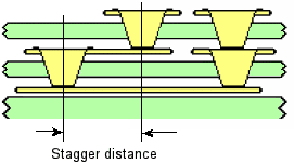
Allow Stacked Micro-Vias allows centre aligned micro-vias on adjacent layer spans, even when the Stagger distance is not 0. You can automatically insert Stacked Micro-Vias using Composite Spans.
Pad
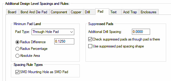
Minimum Pad Land
Select the Pad Type from the drop down list to see or edit the value for that type. You can specify different values for Micro-vias, Through Hole (all other pads), Through Mounting Holes and Vias.
Determines the amount of copper that is needed on each drilled pad. Radius Difference is the difference between the radius of the pad and the radius of the drill. Radius Percentage is the percentage difference between the radius of the pad and the radius of the drill. Absolute Area is the minimum area of copper on the pad land.
Suppressed Pads
Define Additional Drill Spacing around the drill hole of suppressed pads. This is in addition to the spacing derived between the pad item (Pad, Mounting Hole or Via) and the other item. This is instead of the other two check box options below.
The Additional Drill Spacing is also used to determine if a pad can be suppressed when adjacent to copper on the same net. This spacing is the minimum distance between the drill hole and copper on the same net, before the pad will be suppressed.
Check suppressed pads as though pad is there. Check this option to cause design rules checking to still maintain the space around suppressed pads as though the pad were there. This means that you cannot use the additional space created by the pad suppression, but does ensure that there are no extra manufacturing problems caused by tracks which are too close to the drill hole.
Use suppressed pad spacing shape. Check this option to cause design rules checking to still maintain the space around suppressed pads where a spacing shape exception is defined is that layer.
Spacing Rule Types
SMD Mounting Hole as SMD Pad. Check this option to cause design rules checking to use the SMD Pad spacings for a SMD Mounting Hole (i.e. a mounting hole that is only on one side and not drilled). Otherwise a SMD Mounting Hole uses the spacings for a Mounting Hole.
Text
Minimum Text Size
The minimum size of text in the design.

Acid Trap
Acid Trap
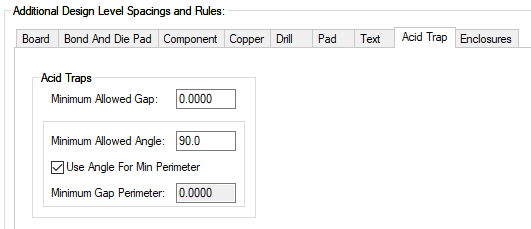
Defines the parameters used to check for Acid Traps and Track Corner Acid Traps when running those DRC options.
The Minimum Allowed Gap is the shortest distance apart two pieces of copper can be without producing an acid trap. If they are closer than this then the Acid Trap check should detect a design rule error. Setting a gap of 0 disables this check.
The Minimum Allowed Angle is defined between track segments or between the edge of a track segment and the pad shape it exits from. An angle of 0 disables this check. An angle greater than 90 degrees will only apply to track segments and not the exit angle from a pad.
The Use Angle For Min Perimeter would be selected if you wish the system to calculate the Minimum Gap Perimeter based on the Minimum Allowed Angle.
The Minimum Gap Perimeter is calculated if Use Angle For Min Perimeter is selected. With this not selected, you can type the perimeter value that you choose.
If using an external program such as Valor for post design DFM checking, this parameter should be directly taken from the value defined in the Valor system.
Enclosures
This tab is for defining the rules used for clash detection within the 3D Viewer environment. Separate values are available for both Board and Components.
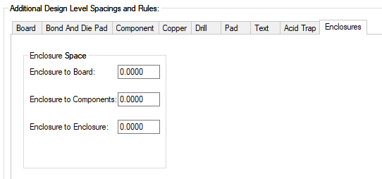
Enclosure Space
Enclosure to Board specifies the STEP model defined as the enclosure and the spacing to any board outline in the design. Boards Cutouts are also taken into consideration during checking and clash detection.
Enclosure to Components is the value used to check between the enclosure and the STEP model defined for a component. If the STEP model is not available, the 3D Package will be used.
Enclosure to Enclosure is the value used to check between multiple enclosures in your design.
Panel
The Panel Rules section is only shown when editing a Panel Design, Panel Profile or PCB Technology file.
V-Score Lines
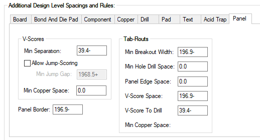
V-Scores are either horizontal or vertical. The minimum separation between parallel V-Scores is defined by the V-Score Min Separation. This separation is from the centreline as they have do physical width. V-Scores can cross each other. The parallel distance from the Panel edge is also defined by the Panel Border spacing, but note that a V-Score can go right up to a perpendicular Panel edge.
Select the Allow Jump-Scoring box if Jump Scores are allowed, this is where the cutter is lifted and brought back down again along its path inside the panel. The minimum end to end distance between V-Scores is defined by the Min Jump Gap, this can be closer than the parallel separation.
Min Copper Space - use this rule to define the minimum spacing between V-Score lines and copper.
Panel Border
Panel Border defines the minimum distance from the panel edge for all the PCB designs. You can put copper, text or other features, which are not within a PCB design, closer to the edge. This spacing also applies to the inside edge of Tab-Routs and the centreline of V-Scores.
The Min Board To Board spacing (see Board section) would normally be set to zero if using V-Scoring or the Tab-Rout line width (i.e drill size used to mill it) if using Tab-Routs.
Tab-Routs
The end to end gaps between Tab-Routs forms the actual tab, this gap must be at least the Min Breakout Width. The inside edge of Tab-Routs must also be the Panel Border distance within the Panel.
The Min Hole Drill Space defines how far apart the small drill holes must be that form a perforation in the breakout tab.
Panel Edge Space - this defines the minimum space required between Tab Routs and the edge of the panel. This will enable you to detect whether the Tab Rout is routing outside the panel outline.
V-Score Space - use this rule to define the minimum space required between Tab Routs and V-Score lines.
V-Score To Drill - this rule defines the minimum V-Score line to drill spacing. This is particularly useful if you have a Tab Routs that use ‘mouse’ bites that are placed near to a V-Score line. It will also be used as your spacing rule when you insert a Tab Rout on a board outline. If mouse bit holes are too close, they will be removed.
Min Copper Space - use this rule to define the minimum spacing between Tab Routs and copper.
Export and Import CSV
Use the Export CSV button to export the data in your PCB design into a CSV format file. Using the Export CSV option will provide you with a formatted template ready for you to edit in your own data. This button is also available within the Panel Editor and has additional fields for the Design Level Spacing Rules and Panel rules.
Use the Import CSV button to import data into the PCB design using a CSV format file. This button is also available within the Panel Editor and has additional fields for the Design Level Spacing Rules and Panel rules.
The data in the file represents a spreadsheet of dialog contents with the data headings along the top row.
Units
The Units button allows you to locally switch between Metric and Imperial units whilst in this dialog. Once the dialog is closed, the units revert back to the original design units. If switching to different units to the design units, the value typed will be converted when you next enter this page.
Related Topics
Technology Overview | Spacing Rules Overview | Net Class Level | Match Pair Level | Check Spacing Values | Importing Class To Class Spacings | Design Rule Check | 3D Viewer | Nets Page | Export CSV | Import CSV