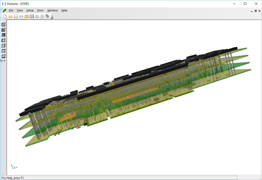
You can choose to show an exploded view representation of your PCB design. This is a 3D view of your board with separation between the layers to show its internal structure.
Enabling this option
This feature is enabled selecting the Show Exploded View of Layer Stack option in the 3D Settings dialog.

Parameters on the 3D Settings dialog allow an Additional Thickness for the Substrate which represent the board, the Layer Drawing Thickness allowed for each layer of information (copper, silkscreen, etc) and the Gap thickness for the Exploded View in the Preview. These are explained in more detail on the 3D Settings page.
It is possible to choose which layers are included in the Exploded View by using the 3D Settings Layers dialog.
Enclosures are not shown in the Exploded View as they are not appropriate and will cause possible clash errors.
If the Show Exploded View of Layer Stack option is enabled then the exploded view is also the view that will be written out to a STEP Output file if one is generated.