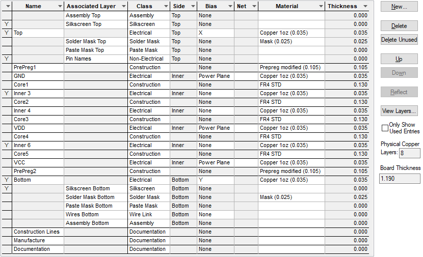
Layers define the parameters of the layers in the design and their position in relation to each other in the physical layer stack. The Name column shows the names of the Electrical and Documentation layers. The Associated Layer column shows the names of the Non-Electrical layers associated with the Electrical layers.
Shortcuts
Menu: Setup
Default Keys: T
Command: Technology
Locating this option
Available from: Setup menu > Technology > Layers tab
Using the dialog
On selection, the Technology dialog opens, select Layers. The existing Layers for the Technology being used will be presented.

Information on Layers is presented in the order that the Layers will exist in the physical board.
In the grid, the Y before the Layer Name shows that the layer is used in the design. The used status is also indicated for the selected style in the editing pane with the Used box showing a ‘tick’.
Navigation
The buttons to the right side of the dialog are used to navigate the grid, the general common buttons are detailed on the Technology Navigation page.
The Up and Down buttons are used to position and move the selected layer in the grid. These are useful to move layers around especially when trying to position them for better visibility in the design (the order looking down the list is how they will be presented in the design).
The Reflect button is used to create the second half of the layer stack by mirroring the first half. Documentation and Drill Drawing layers are not taken into account, and will remain at the bottom of the grid.
If you already have a Top and Bottom electrical layer, and the bottom electrical layer is not used in the design, then the top electrical layer will be reflected and will replace the bottom electrical layer. If it is used in the design, the layer will not be changed (this is true for all layer classes).
The View Layers button takes you to the Layer Stack Preview dialog, which offers a simple view of the layer stack.
Use the Only Show Used Entries check box below the layers list to specify if layers that do not contain any design items should be included in the list.
The Physical Copper Layers is displayed at the bottom of the dialog. This is the count of electrical layers that have Physical Copper Layer set in their Layer Class.
The total Board Thickness will be shown at the bottom of the dialog if any layers have a thickness defined. Layers that are defined as being embedded will not have their thickness included in the total unless they are on the top side and embedded upwards, or on the bottom side and embedded downwards.
Using the editing pane

The following describes each parameter defined in the dialog:
Name
A Layer must have a Name which must be unique and is the string used to refer to the Layer throughout the system.
Class
The Layer Class defines what type of layer it is, the selection is chosen from a predefined (user definable) list that has been created in the Layer Class dialog. This determines what type of items can appear on the layer, and how they will appear.
Type
The Type of the chosen layer class is displayed underneath the class (sometimes with extra information from the class next to it).
Note: once a layer has been used in the design you can only change the class to one of the same type.
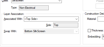
Layer Association
Normally, you will have a Top, a Bottom and a number of Inner Electrical layers.
You will usually associate some Non-Electrical layers with the
The Swap With field, shows the other layer the current layer will swap with. This will be available for non-electrical layers. This is usually the layer on the opposite side which is associated with the same layer class. If the current layer does not have an equivalent for the other side, it is possible to nominate another layer from the opposite side to swap with. This allows you to have different layer class settings on each side.

Using ‘Can Have Associated Layers’ and why
For more advanced technologies, you may want to associate Non-Electrical layers to Inner layers. To do this, edit the inner electrical layer and check the Can Have Associated Layers box.
Once enabled, you can define which way the layer faces, normally electrical layers will be in top and bottom facing pairs.
You can also allow Normal or Buried components on to the layer. The way the layer faces will determine if the component is mirrored.
Once an electrical layer can have associated layers, you can associate Non-Electrical layers
by editing them and selecting the
For particular uses of the Facing and Allow Components options for inner layers, see the sections on Micro-vias, Embedded Components and Flexi-Rigid Boards & Boards with Cavities below.
For Drill Drawing layers,
you should associate a Layer Span. You
should also specify what types of Drill Holes should be displayed (Plated / Non Plated, Round /
Non Round). The Drill Drawing letters and symbols
will appear on this layer appropriate to the drilled pads, vias, etc which are in the design.
You can override the default position of the drill letter for an individual pad by adding a
Electrical Details
This section only applies to Electrical layers.
Routing Bias
The Routing Bias helps Automatic Routing determine the routing pattern on that layer. For normal routing layers it is best to alternate X and Y bias. This helps to form channels of tracks which normally leads to a neater and more dense routing pattern.
- None means there is no X or Y bias on this layer, so tracks can go in any direction.
- X means that tracks should predominantly be in the X (horizontal) direction.
- Y means that tracks should predominantly be in the Y (vertical) direction.
- Minimum Tracks means that only where necessary should tracks be on this layer. This would normally be used for an outer electrical layer with surface mounted components. On such layers, tracks are necessary to exit the pads, but long tracks would be undesirable.
- No Autoroute means no Automatic Routing on this layer. You can use this to disable a layer for Automatic Routing.
- No Tracks also means no Automatic Routing on this layer, but in addition any tracks added interactively on this layer will be flagged as in error by the Design Rule Check - Track Layer option.
- Power Plane means that the layer would normally be photo-reversed for post processing. Automatic Routing will not put any tracks on this layer, but would put vias down to to connect to the signal it carries. This option is normally combined with the Net Name parameter to produce a full power plane. Split Power Planes are also possible.
Note: an electrical layer that is not a physical copper layer (see Layer Class) will have its bias forced to No Tracks.
Power Plane Net
The Power Plane Net Name provides the signal carried by this layer. The layer therefore becomes a full power plane so Vias and Pads can connect to this layer. With a Routing Bias Set to Power Plane and no Power Plane Net name defined, the plane still has special power plane properties but now expects the net association to be supplied using one or more Copper Pour Templates acting as split planes.
Construction Details
To fully document your layer stack, you can optionally define the Material and Thickness of a layer.
Material
Choose the material from which the layer is made. You can only choose a material that has previously been defined in the Materials dialog. The New Material button enables you to easily navigate to this page to create a new material if the required one does not exist.
Thickness
The Thickness of the Material, in the current design units. By default, this thickness is taken from the Material, but you can define a specific value for this layer by checking the Thickness box and typing in a value. This can be done without having to set a material name.
Embedding
Define if the current layer embeds itself Upwards into the layer above, or Downwards into the layer below.
Check boxes
Usually Plotted
Defines if the current layer would normally be plotted, if you uncheck this option, then a plot will not be generated for this layer, or appear in the list of layers requiring a plot. It does not prevent you from manually creating a plot.
Note: an electrical layer that is not a physical copper layer (see Layer Class) will have Usually Plotted forced to off.
In Layer Stack Preview
Defines if the current layer will appear in the Layer Stack Preview. A layer that is either the From Layer or To Layer in a Layer Span, or the Stop Layer in a Back Drill Span is required in the Layer Stack Preview, and so this check box will be disabled and automatically checked.
Export and Import
Use the Export CSV button to export the layers in your PCB design into a CSV format file.
Use the Import CSV button to import layers into the PCB design using a CSV file or XML format file. A file created in IPC-2581 format would be saved with a .xml file extension. This format is used for more complex layer structures created in external products and may have been impedance verified for example.
The data in the file represents a spreadsheet of layers with the layer data headings along the top row.
Units
The Units button allows you to locally switch between Metric and Imperial units whilst in this dialog. Once the dialog is closed, the units revert back to the original design units. If switching to different units to the design units, the value typed will be converted when you next enter this page.
Special Layer considerations

Micro-vias
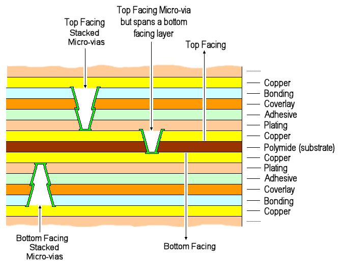
If you are using a Micro-via technology, you will need to enable Can Have Associated Layers, to be able to define if the layer is Top Facing or Bottom Facing. You can then define a suitable Layer Span.
Special Micro-vias
A Micro-via is usually defined between two top or two bottom facing layers. You can create a special exception to this rule by checking the Allow Micro-via Stop Pad Either Side option on a inner electrical layer. You will be prompted to confirm that you are able to manufacture this micro-via technology. This will allow you to create micro-vias onto the inner electrical layer from above or below, regardless of the facing value of this layer. You should only use this if you really know what you’re doing and following consultation with your manufacturer.
In the example below, using this setup enables a layer span like this to be created where a Micro-via can be added as top facing but will span to a bottom facing layer.

Embedded Components
Special technologies such as those using Embedded Components (for example printed resistors) are created by enabling the Can Have Associated Layers on an Inner Electrical layer. This enables you to associate Non-Electrical layers with that inner layer to define the manufacturing processes required. Enabling the Allow Buried Components option on the Inner layer allows you to add embedded components to that layer. Finally, the Bottom Facing check box causes components added to this layer to be mirrored.
Flexi-Rigid Boards & Boards with Cavities
A flexi-rigid board is a composite of a flexi-board, with rigid board areas applied to the surface. Components can be attached to the rigid areas and optionally to the exposed flexi-board surface as well. This is achieved by placing the flexi-board on a inner layer span. You can also create board cavities, cutouts that expose an inner layer as a surface. This is done by using a Board Cutout Area on a layer span. Components can then be placed within these cavities.
In both cases you need to allow components to sit on inner layers. To do this, enable the Can Have Associated Layers for the inner layers that are at the top or bottom of the board layer span. Then check the Allow Normal Components option to allow components sit on these layers. You will now be able to use Change Layer to move normal components onto the inner layers. Finally, the Bottom Facing check box causes components added to this layer to be mirrored.
Tented Vias
Tented Vias can be created in Pulsonix. Please refer to the Tented Vias section under the Layer Classes page.
Layer Stiffeners
If your design requires layer stiffeners (for use in a flexi-board for example), then special consideration is required when creating Layer Classes. Please refer to the Technology Layer Classes page for more information.
Related Topics
Technology Overview | Layer Classes | Materials | Net Name | Layer Stack Preview | Colours | Layers Overview | Embedded Components | Suppress Lands Rule | Units | Using Dialog Grids | Import and Export Layers CSV | Import IPC-2581 Layer Stacks