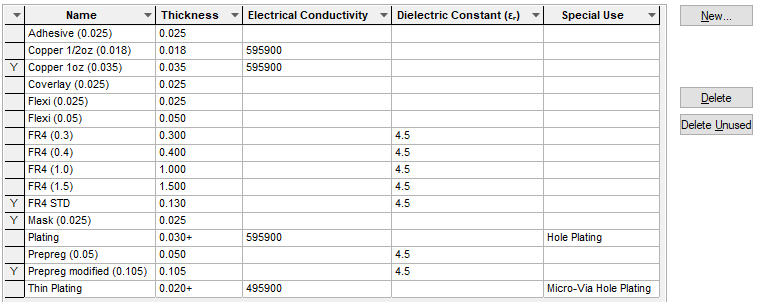
The Materials dialog gives a list of the defined Materials with associated Thicknesses and electrical characteristics.
To fully document the construction of a board you should specify the Materials used in each physical layer. This is not only important for a bill of materials, but may also be used in a physical analysis, such as electro-magnetic field effects and thermal analysis.
Shortcuts
Menu: Setup
Default Keys: T
Command: Technology
Locating this option
Available from: Setup menu > Technology option > Materials tab
Using This Dialog
On selection, the Technology dialog opens, select Materials. The existing Materials for the Technology being used will be presented.

Navigation
The buttons to the right side of the dialog are used to navigate the grid, the general common buttons are detailed on the Technology Navigation page.
Materials Editing Pane
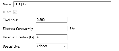
Materials can be edited directly in the grid or by selecting a line in the grid and editing the rule.

A material will normally have a descriptive Name, such as FR4, PrePreg etc. which will indicate its use.
The material Thickness is defined in the current design units, or you can type the units after the thickness, e.g. 0.65mm
The material Electrical Conductivity value quantifies how strongly the material conducts electric current. This is defined using the SI unit of Siemens per metre (S/m). It is the inverse of the Copper Resistivity value used by the Track Width and Resistance Calculator.
The material Dielectric Constant value, also referred to as Er, is the relative permittivity of a material. It is used by the Track Impedance Calculator.
The Special Use parameter specifies if the material has a special use within the system. Hole Plating means the material is used to plate normal holes, and Micro-Via Hole Plating is the material used to plate micro via holes. Each special use type can only be applied to one material. The values on these materials are used by the Via Resistance Calculator.
Units
The Units button allows you to locally switch between Metric and Imperial units whilst in this dialog. Once the dialog is closed, the units revert back to the original design units. If switching to different units to the design units, the value typed will be converted when you next enter this page.
Where Materials Are Used
Any Materials defined can be used within the Layers dialog. If a thickness is defined for a Material, this will be the default thickness for the layer. In the Layers dialog it will contribute to the total Board Thickness calculated for all combined layers within the stack.
The material thickness and other parameters are also used in conjunction with the Track Impedance Rules, as well as Design Calculators for: Track Impedance, Track Width and Resistance, and Via Resistance.
Related Topics
Technology Overview | Technology - Layers | Via Resistance Calculator | Track Impedance Calculator | Track Width and Resistance Calculator